

Page 1
www.fairchildsemi.com
RC2951
Adjustable Micropower Voltage Regulator
Features
• High accuracy output voltage
• Guaranteed 100 mA output current
• Extremely low quiescent current
• Extremely tight load and line regulation
• Requires only a 1.0µF output capacitor for stability
• Internal Current and Thermal Limiting
• Error flag warns of output dropout
• Logic-controlled electronic shutdown
• Output programmable from 1.24 to 29V
• Fixed 3.3V version available
• -25°C to +85°C operating range
• 8 lead SOIC package
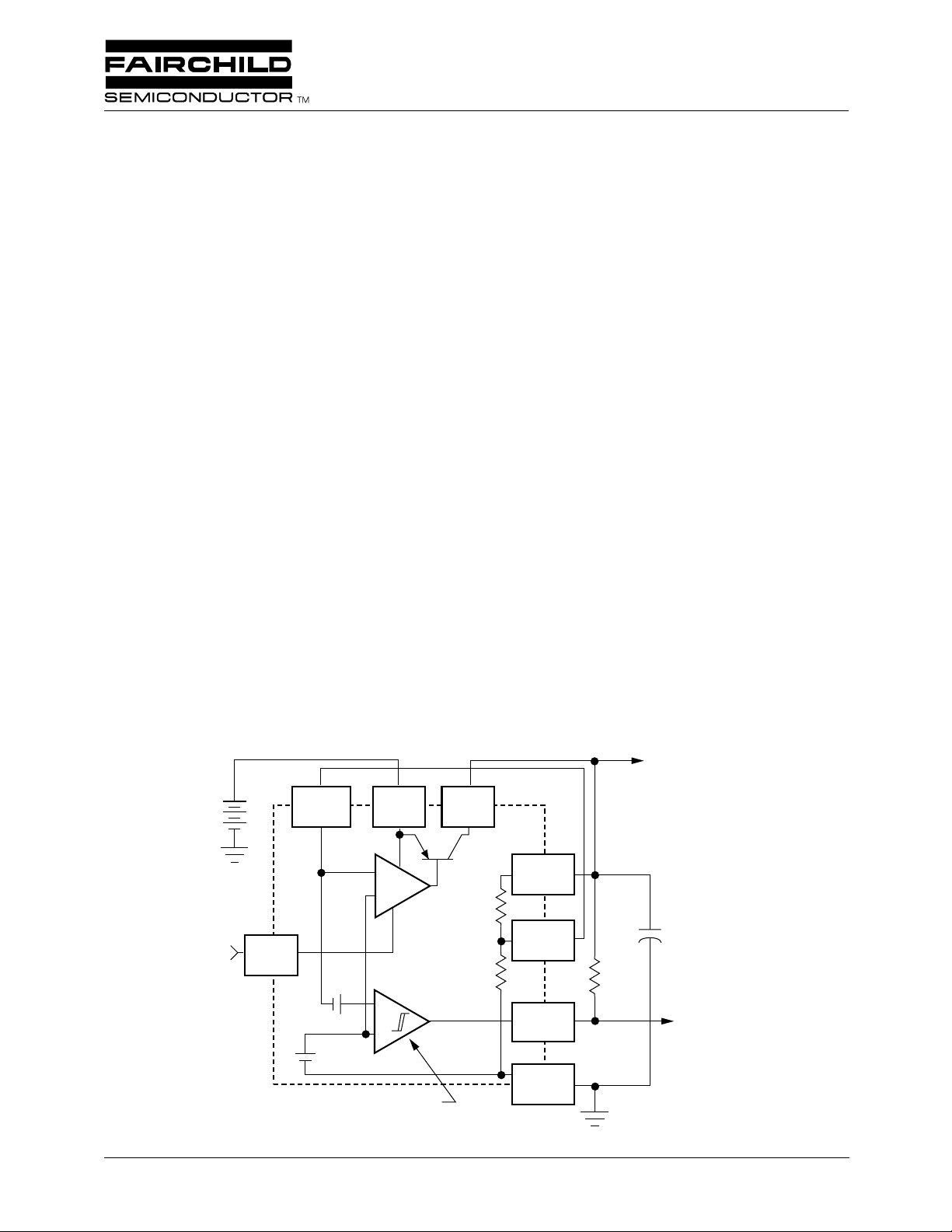
Block Diagram
Description
The RC2951 is a voltage regulator specifically designed to
maintain proper regulation with a very low dropout voltage
(Typ. 40mV at light loads and 380 mV at 100mA). It has a
low quiescent bias current of 75µA and is capable of supplying output currents in excess of 100mA. It has internal current and thermal limiting protection. The output can be
programmed from 1.24V to 29V with two external resistors.
A fixed output voltage (3.3V) is also available.
The error flag output can be used as power-on reset for
warning of a low output voltage. The Shutdown input feature
allows a logic level signal to turn on and off the regulator
output. The RC2951 is ideally suited for battery powered
computer, consumer, and industrial equipment where an
extension of useful battery life is desirable. The RC2951 is
available in an 8-pin SOIC package.
V
Unregulated DC
+
From
CMOS
or TTL
PRELIMINARY INFORMATION describes products that are not in full production at the time of printing. Specifications are based on design goals
and limited characterization. They may change without notice. Contact Raytheon for current information.
3
Shut
Down
781
Feed-
Back
60 mV
+
1.23V
Reference
Error Detection Comparator
Input Output
+
–
Error
Amplifier
+
+
–
Sense
V
Error
Ground
IL ≤ 100 mA
2
6
TAP
5
4
OUT
+
See Application
Discussion
330kΩ
To CMOS
or TTL
REV. 1.0.1 4/8/02
Page 2
RC2951 PRODUCT SPECIFICATION
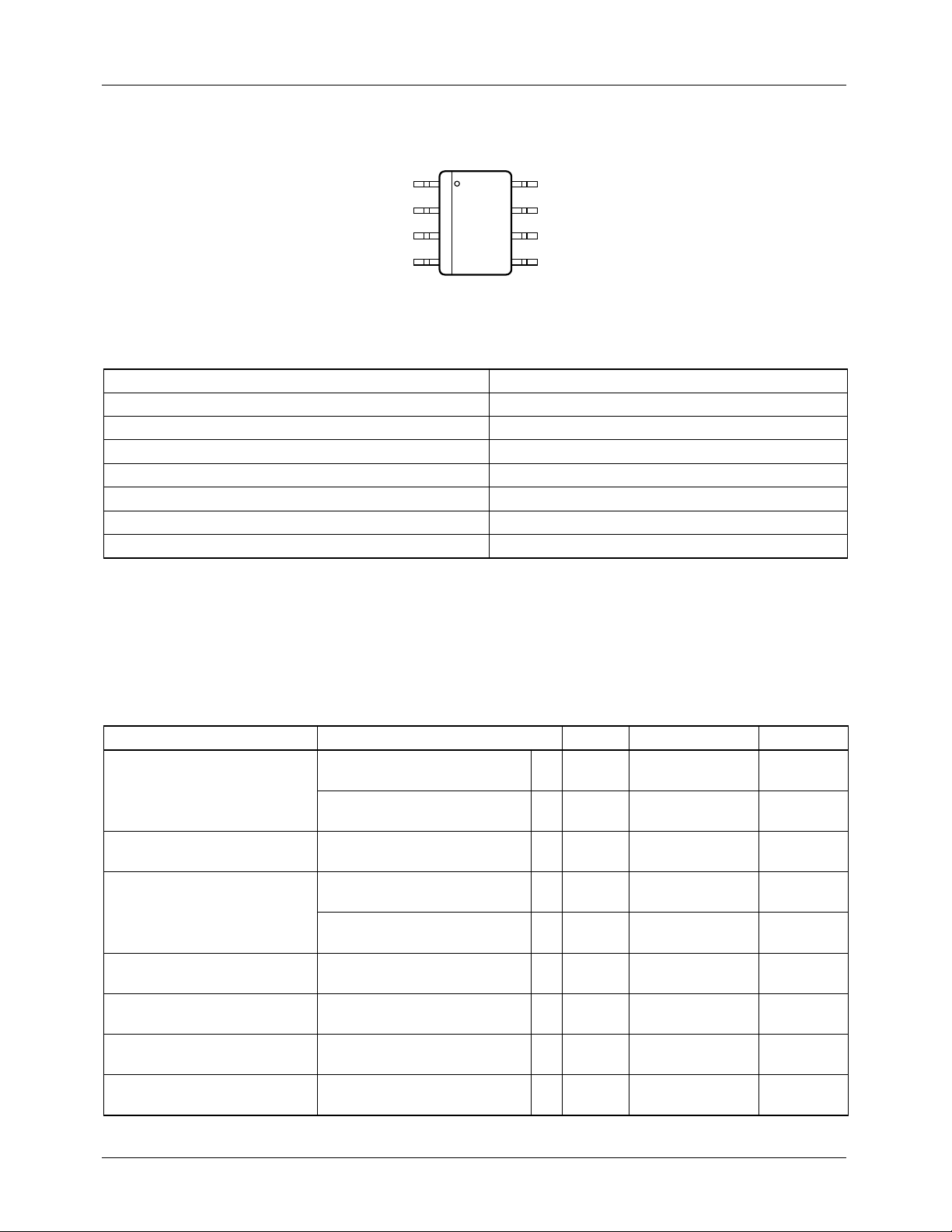
Pin Assignments
8 Lead SOIC Package
Output
Sense
Shutdown
Ground
1
2
3
4
Input
8
Feedback
7
V
6
5
TA P
Error
Top View
Absolute Maximum Ratings
Power Dissipation Internally Limited
Lead Temp. (Soldering, 5 seconds) 260°C
Storage Temperature Range –65° to +150°C
Operating Junction Temperature Range
Input Supply/Voltage –0.3 to +30V
Feedback Input Voltage
Shutdown Input Voltage
2,3
2
Error Comparator Output Voltage
Notes:
1. Junction to ambient thermal resistance for the S.O. (M) package is 160°C/W.
2 May exceed input supply voltage.
3. When used in dual-supply systems where the output terminal sees loads returned to a negative supply, the output voltage
should be diode-clamped to ground.
1
–55° to +150°C
–1.5 to +30V
–0.3 to +30V
2
–0.3 to +30V
Electrical Characteristics
The • denotes that the limits apply at temperature extremes.
Parameter Conditions
Output Voltage
TJ = 25°C 5.0 5.025
(RC2951M)
-25°C ≤ TJ ≤ 85°C •
Output Voltage
(RC2951M)
Output Voltage
100µA ≤ IL ≤ 100mA
TJ ≤ T
TJ = 25°C 3.3 3.317
(RC2951M-3.3)
-25°C ≤ TJ ≤ 85°C •
Output Voltage
(RC2951M-3.3)
Output Voltage Temperature
Coefficient
Line Regulation
Load Regulation
7
9, 10
9
100µA ≤ IL ≤ 100mA
TJ ≤ T
(VONOM + 1)V ≤ Vin ≤ 20V
100 µA ≤ IL ≤ 100 mA
1
JMAX
JMAX
Typ. Tested Limit
2
Units
V max
5.0 5.06
•
•
5.0 5.075
•
4.975
4.94
4.925
V min
V max
V min
V max
V min
V max
3.3 3.340
•
•
3.3 3.346
•
3.284
3.260
3.254
V min
V max
V min
V max
V min
• 20 120 ppm/°C
0.03 0.1
•
0.08 0.2
•
0.5
0.4
% max
% max
% max
% max
2 REV. 1.0.1 4/8/02
Page 3
PRODUCT SPECIFICATION RC2951
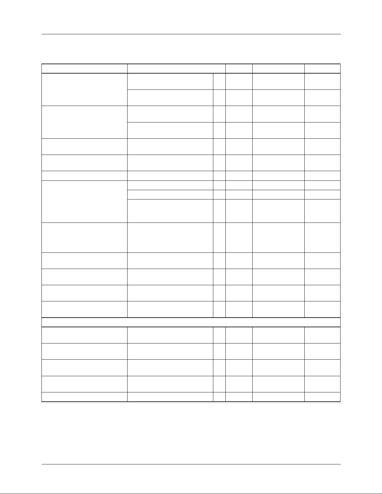
Electrical Characteristics (continued)
The • denotes that the limits apply at temperature extremes.
Parameter Conditions
Dropout Voltage
Ground Current I
Dropout Ground Current V
3
IL = 100 µA
= 100 mA
I
L
= 100 µA
L
= 100 mA
I
L
= (VONOM - 0.5)V
in
IL = 100 µA •
Current Limit V
Thermal Regulation
8
Output Noise,
10 Hz to
100 KHz
= 0
out
CL = 1 µF (5V Only) 430 µV rms
CL = 200 µF 160 µV rms
CL = 3.3 µF
(Bypass = 0.01 µF
Pins 7 to 1 (RC2951)
Reference Voltage
Reference Voltage
5
Feedback Pin Bias Current
Reference Voltage
Temperature Coefficient
7
Feedback Pin Bias Current
Temperature Coefficient
Error Comparator
Output Leakage Current VOH = 30V
Output Low Voltage V
= (VONOM - 0.5)V
in
IOL = 400 µA •
Upper Threshold Voltage
Lower Threshold Voltage
Hysteresis
4
4
4
1
Typ. Tested Limit
50 80
•
150
380 500
•
700
75 120
•
140
81415mA max
•
110 250
300
160 200
•
220
0.05 0.2 %/W max
100 µV rms
1.235 1.25
•
1.26
1.22
•
•
•
1.2
1.27
1.19
20 40
•
60
20 ppm/°C
0.1 nA/°C
0.01 1
•
150 250
400
60 40
•
25
75 95
•
140
15 mV
2
Units
mV max
mV max
mV max
mV max
µA max
µA max
mA max
µA max
µA max
mA max
mA max
V max
V max
V min
V min
V max
V min
nA max
nA max
µA max
2
µA max
mV max
mV max
mV min
mV min
mV max
mV max
REV. 1.0.1 4/8/02 3
Page 4
RC2951 PRODUCT SPECIFICATION
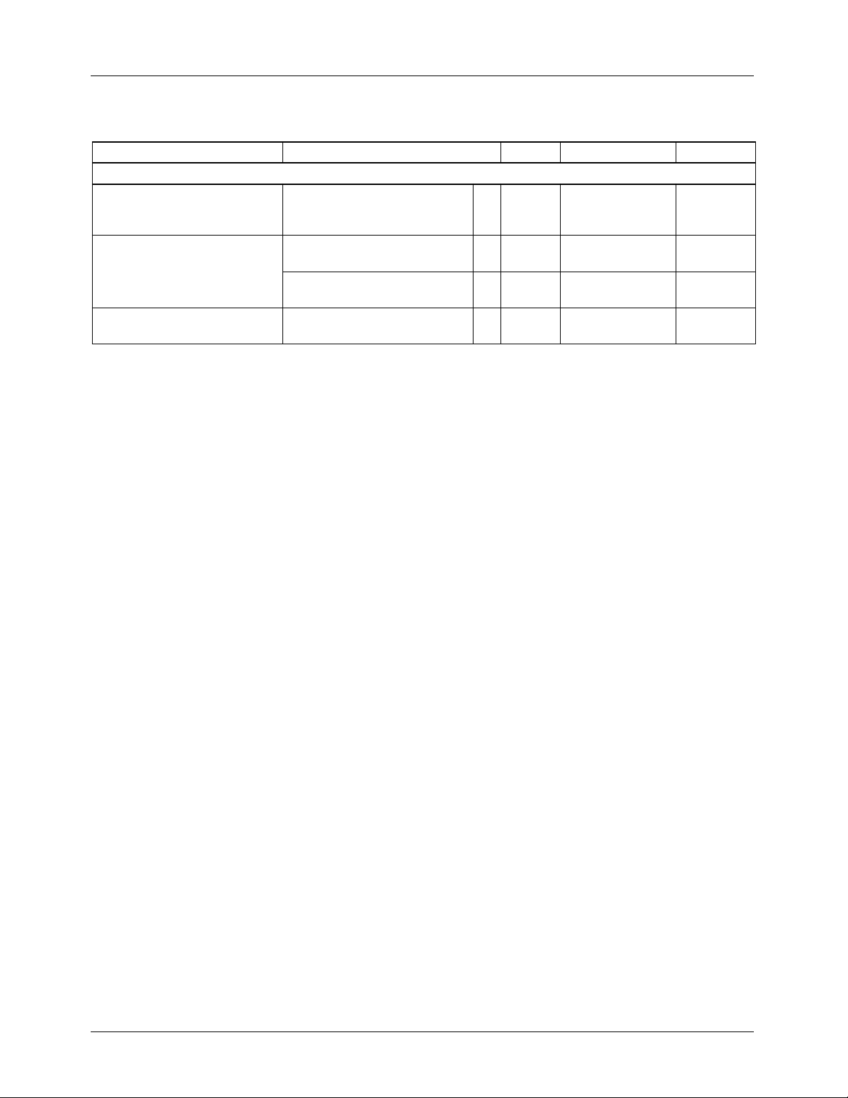
Electrical Characteristics (continued)
The • denotes that the limits apply at temperature extremes.
Parameter Conditions
1
Typ. Tested Limit
Shutdown Input
Input Logic Voltage
Low (Regulator ON)
High (Regulator OFF)
Shutdown Pin Input Current V
Regulator Output
Current in Shutdown
Notes:
1. Unless otherwise specified all limits guaranteed for T
versions, and 2.2 µF for 3V and 3.3V versions. Additional conditions for the 8-pin versions are Feedback tied to V
Output tied to Output Sense and V
2. Guaranteed and 100% production tested.
3. Dropout Voltage is defined as the input to output differential at which the output voltage drops 100 mV below its nominal value
measured at 1V differential. At very low values of programmed output voltage, the minimum input supply voltage of 2V (2.3V
over temperature) must be taken into account.
4. Comparator thresholds are expressed in terms of a voltage differential at the Feedback terminal below the nominal
reference voltage measured at V
by the error amplifier gain = V
is guaranteed to go low when the output drops by 95 mV x 5V/1.235V = 384 mV. Thresholds remain constant as a percent
of V
as V
out
out
5. V
< V
ref
6. V
shutdown
7. Output or reference voltage temperature coefficient is defined as the worst case voltage change divided by the total
temperature range.
8. Thermal regulation is defined as the change in output voltage at a time T after a change in power dissipation is applied,
excluding load or line regulation effects. Specifications are for a 50 mA load pulse at V
T = 10 ms.
9. Regulation is measured at constant junction temperature, using pulse testing with a low duty cycle. Changes in output voltage
due to heating effects are covered under the specification for thermal regulation.
10. Line regulation for the RC2951 is tested at 150°C for I
by design to 0.2%. See Typical Performance Characteristics for line regulation versus temperature and load current.
≤ (V
out
≥ 2V, Vin ≤ 30V, V
6
is varied, with the dropout warning occurring at typically 5% below nominal, 7.5% guaranteed.
– 1V), 2.3V ≤ Vin ≤ 30V, 100µA ≤ IL ≤ 100 mA, TJ ≤ T
in
shutdown
V
shutdown
shutdown
= (VONOM + 1)V. To express these thresholds in terms of output voltage change, multiply
in
out/Vref
= 0, Feedback pin tied to V
out
= 2.4V
= 30V
= 25°C, Vin = (VONOM + 1)V, IL = 100µA and CL = 1 µF for 5V
J
< 0.8V.
= (R1 + R2)/R2. For example, at a programmed output voltage of 5V, the Error output
JMAX
.
TAP
= 1 mA. For IL = 100 µA and TJ = 125°C, line regulation is guaranteed
L
1.3
•
•
30 50
•
450 600
•
31020µA max
•
.
0.6
2.0
100
750
= 30V (1.25W pulse) for
IN
2
Units
V
V max
V min
µA max
µA max
µA max
µA max
µA max
,
TAP
4 REV. 1.0.1 4/8/02
Page 5
PRODUCT SPECIFICATION RC2951
Applications Discussion
The RC2951 regulator is designed with internal current limiting and thermal shutdown. It is not internally compensated
and requires a 1.0µF (or greater) capacitor between the output terminal and ground for stability. At lower output voltages, more capacitance is required (2.2µF or more is
recommended for 3V and 3.3V versions) for stability. Most
types of aluminum, tantalum or multilayer ceramic capacitors will perform adequately. Solid tantalums or appropriate
multilayer ceramic capacitors are suggested for operation
below 25°C. At lower values of output current, less capacitance is needed to maintain stability at output. The capacitor
at the output can be reduced to 0.33µF for currents less that
10mA, or 0.1µF for currents below 1.0mA.
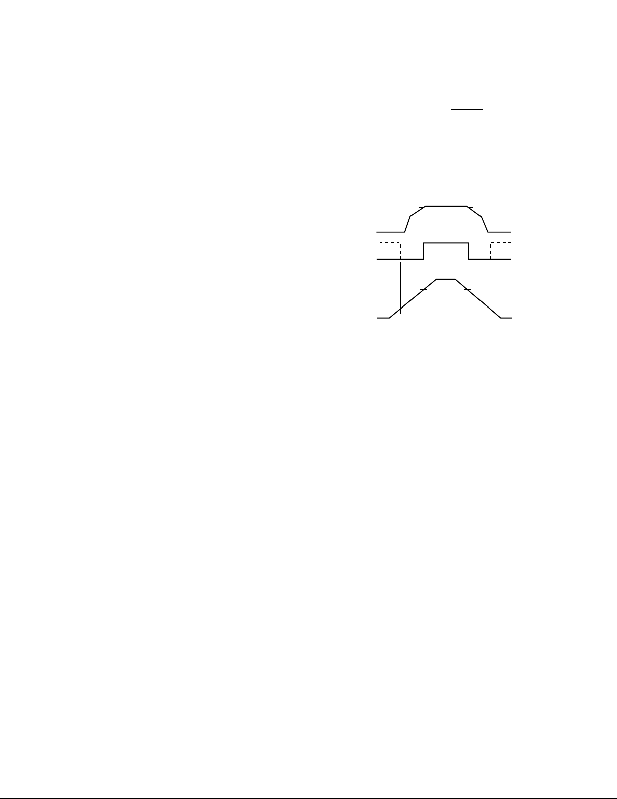
Figure 1 is a timing diagram showing the ERR
OR signal and
the regulated output voltage as the RC2951 input is ramped
up and down. For 5V versions, the ERR
OR signal becomes
valid (low) at about 1.3V input. It goes high at about 5V
input (the input voltage at which V
= 4.75.) Since the
OUT
RC2951’s dropout voltage is load-dependent (see curve in
typical performance characteristics), the input voltage trip
point (about 5V) will vary with the load current. The output
voltage trip point (approx. 4.75V) does not vary with load.
Output
Voltage
4.75V
Using the adjustable versions at voltages below 5V runs the
error amplifier at lower gains so that more output capacitance is needed. For the worst-case situation of a 100 mA
load at 1.23V output (Output shorted to Feedback) a
3.3 µF (or greater) capacitor should be used.
When setting the output voltage of the RC2951 versions with
external resistors, a minimum load of 1 µA is recommended.
A 1 µF tantalum or aluminum electrolytic capacitor should
be placed from the RC2951 input to ground if there is more
than 10 inches of wire between the input and the AC filter
capacitor or if a battery is used as the input.
Stray capacitance to the RC2951 Feedback terminal can
cause instability. This may especially be a problem when
using high value external resistors to set the output voltage.
Adding a 100 pF capacitor between Output and Feedback
and increasing the output capacitor to at least 3.3 µF will fix
this problem.
Error Detection Comparator Output
The comparator switches to a logic low whenever the
RC2951 output falls out of regulation by more than approximately 5%. This value is the comparator’s built-in offset of
about 60 mV divided by the 1.235 internal reference voltage.
This trip level remains “5% below normal” regardless of the
value of the output voltage. For example, the error flag trip
level is typically 4.75V for a 5V output or 11.4V for a 12V
output. The out of regulation condition may be due either to
low input voltage, current limiting, or thermal limiting.
Error*
Input
Voltage
Figure 1. ERROR
5V
1.3V
2950-10
Output Timing
The error comparator has an open-collector output which
requires an external pullup resistor. This resistor may be
returned to the output or some other supply voltage depending on system requirements. In determining a value for this
resistor, note that while the output is rated to sink 400 µA,
this sink current adds to battery drain in a low battery condition. Suggested values range from 100k to 1MΩ. The resistor
is not required if this output is unused.
Programming the Output Voltage (RC2951)
The RC2951 may be pin-strapped for the nominal fixed
output voltage using its internal voltage divider by tying the
output and sense pins together, and also tying the feedback
and V
for any output voltage between its 1.235V reference and its
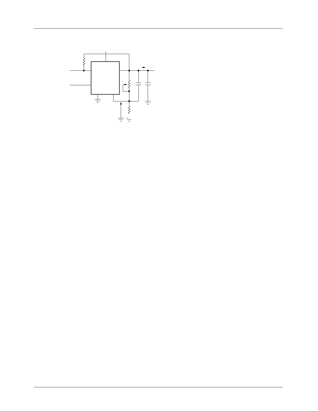
30V maximum rating. As seen in Figure 2 an external pair of
resistors is required.
pins together. Alternatively, it may be programmed
TA P
REV. 1.0.1 4/8/02 5
Page 6
RC2951 PRODUCT SPECIFICATION
V
OUT
V
REF
R1R2+
R
2
-------------------
=
.
+V
IN
Error
Output
**Shutdown
Input
100K
5
3
8
+V
IN
ERROR
RC2951
SD
GND FB
V
OUT
1.2 30V
1
V
OUT
V
74
REF
1.23V
++
R
1
R
2
.01
µF
3.3µF
2950-11
V
OUT
V
=
REF
** Drive with TTL-high to shut down. Ground or leave open if shutdown feature is not to be used.
Figure 2. Adjustable Regulator
The complete equation for the output voltage is
R
1
V
REF
OUT
1
------+
IFBR
+•=
R
2
V
OUT
V
REF
-------------R
2
V
-------------------=
R1R2+
1
Reducing Output Noise
In reference applications it may be advantageous to reduce
the AC noise present at the output. One method is to reduce
the regulator bandwidth by increasing the size of the output
capacitor.
Noise can be reduced fourfold by a bypass capacitor across
R1, since it reduces the high frequency gain from 4 to unity.
Pick
V
OUT
=
V
1
REF
Adding the error term,
V
OUT
V
1
REF
R
1
------+
R
2
C
BYPASS
or about 0.01 µF. When doing this, the output capacitor must
be increased to 3.3 µF to maintain stability. These changes
R
1
------+
IFBR
+=
R
2
2
reduce the output noise from 430 µV to 100 µV rms for a
100 kHz bandwidth at 5V output. With the bypass capacitor
added, noise no longer scales with output voltage so that
------------------------------------
≅
2πR
improvements are more dramatic at higher output voltages.
where V
is the nominal 1.235 reference voltage and IFB
REF
is the feedback pin bias current, nominally -20 nA. The
minimum recommended load current of 1 µA forces an
upper limit of 1.2 MΩ on the value of R2, if the regulator
must work with no load (a condition often found in CMOS in
standby). IFB will produce a 2% typical error in V
OUT
which
may be eliminated at room temperature by trimming R1.
For better accuracy, choosing R2 = 100k reduces this error
to 0.17% while increasing the resistor program current to
12 µA. Since the RC2951 typically draws 60 µA at no load
with Pin 2 open-circuited, this is a small price to pay.
R
1
1
------+
R
2
1
200Hz•
1
6 REV. 1.0.1 4/8/02
Page 7
PRODUCT SPECIFICATION RC2951
Typical Applications
Unregulated
Input
1µF
6
V
TAP
7
FB
1MΩ
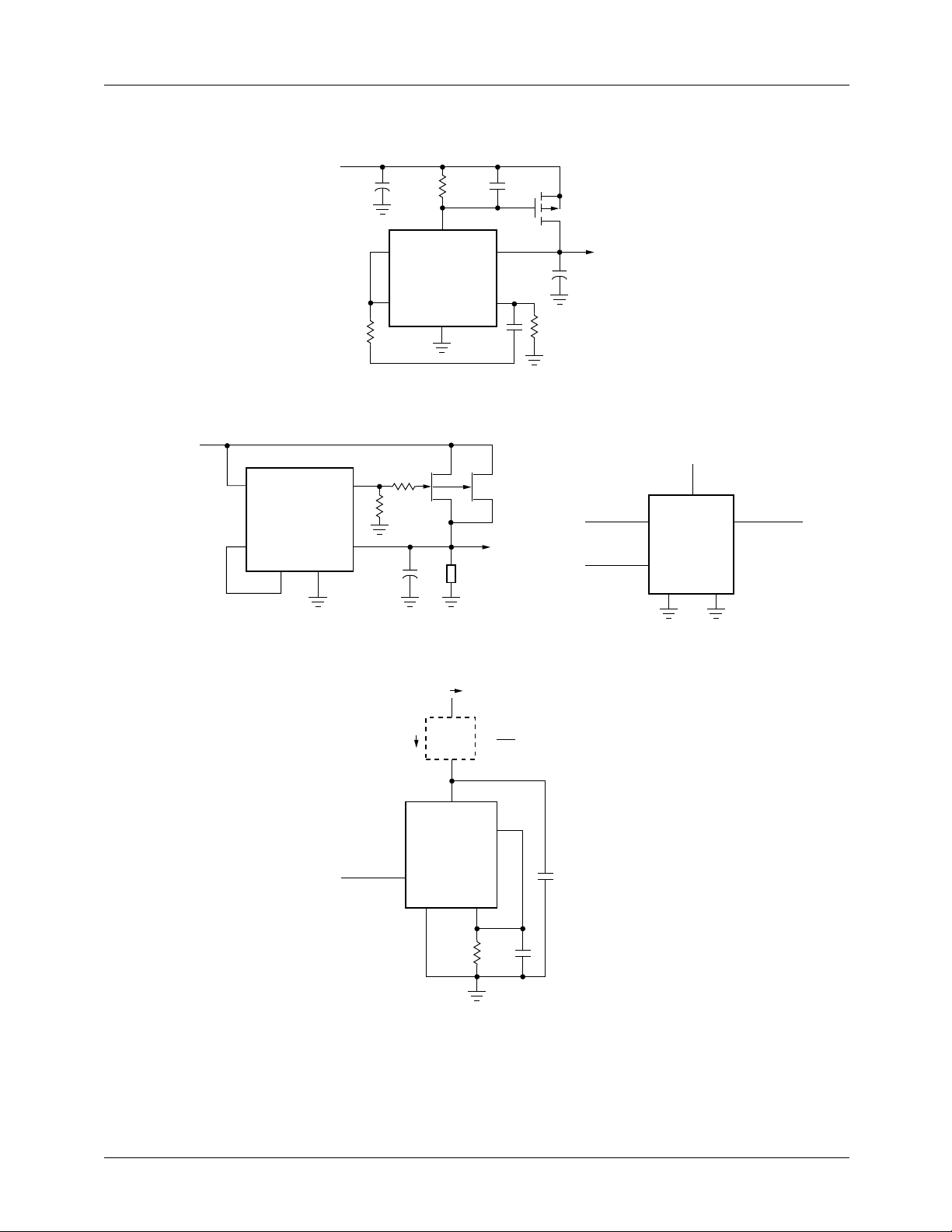
Figure 3. 1A Regulator with 1.2V Dropout
10kΩ
8
IN
RC2951
GND
4
0.01µF
SENSE
OUT
0.002µF
Supertex
VP12C
+
220µF
I
400µA
Q
Output
5V±1%@
0 to 1A
2
1
2kΩ
Unregulated
Input
8
IN
RC2951
6
V
TAP
GNDFB
7
OUT
SENSE
4
1
2
4.7µF
27kΩ
+
Load
50mA to
300mA
330Ω
Figure 4. 300 mA Regulator with 0.75 Dropout
+V = 2 30V
Load
L
8
V
IN
RC2951
Shutdown
Input
3
SD
GND
4
R
1%
V
FB
IL=I
OUT
7
2N5432
(2)
5V
Output
1.23
R
1
1 µF
+V
IN
8
+V
Error
Output
**Shutdown
Input
*Minimum input-output voltage ranges from
40 mV to 400 mV, depending on load current.
Current limit is typically 160 mA.
Figure 5. Wide Input Voltage Range
0.1µF
+
5
3
Current Limiter
IN
ERROR
RC2951
SD
GND
4
*V
OUT≈VIN
1
V
OUT
FB
4
2950-12
Figure 6. Low Drift Current Source
REV. 1.0.1 4/8/02 7
Page 8
RC2951 PRODUCT SPECIFICATION
Typical Applications (continued)
+V
IN
8
+V
IN
6
V
TAP
RC2951
#1
FB
7
SENSE
V
ERROR
OUT
D
1
2
1
5
+
GND
4
27kΩ
D
2.7MΩ
Q
1
6
7
3
V
FB
SD
+V
TAP
8
IN
RC2951
D
4
SENSE
#2
ERROR
V
OUT
3
2
1
5
330kΩ
Main 5V Output
+
GND
4
• Early warning flag on low input voltage
• Main output latches of f at lower input voltages
• Battery backup on auxillary output
Operation Reg. #1’s V
flag becomes active when V
flag of Reg. #2 becomes active and via Q1 latches the main output off.
When V
again exceeds 5.7V Reg. #1 is back in regulation and the early
in
warning signal rises unlatching Reg. #2 via D3.
is programmed one diode drop above 5V. Its error
OUT
≤ 5.7V. WhenVin drops below 5.3V, the error
in
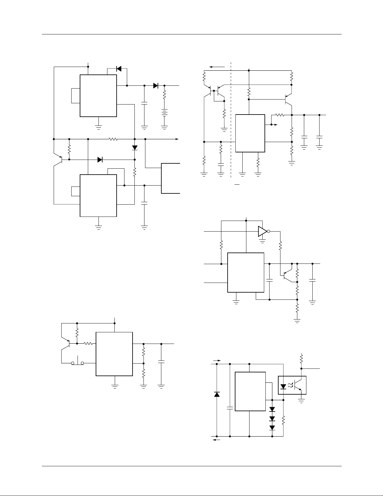
Figure 7. Regulator with Early Warning and Auxillary Output
+V
IN
8
+V
IN
RC2951
GND
1
V
OUT
R
7
FB
R
Reset
470kΩ
470kΩ
5
ERROR
3
SD
4
Figure 8. Latch Off When Error Flag Occurs
5V Memory
D
2
Supply
20
1µF
3.6V
Nicad
EARLY WARNING
RESET
µP
V
DD
1µF
V
OUT
1
+
1µF
2
Current
Limit Section
+V
= V
+5.0V
IN
OUT
680 0.05
470
MJE2955
2N3906
10kΩ
5
Error
Flag
R
1
7
FBSD
1
1%
R
2
47
4.7MΩ
+V
8
IN
ERROR
RC2951
3
V
OUT
220
20kΩ
= 1.23V
V
OUT
,use internal resistors. Wire pin 6 to 7, & wire pin 2 +V
For 5V
OUT
GND
4
.033
R
1
1 +
()
R
2
Figure 9. 2 Ampere Low Dropout Regulator
+V
IN
C-MOS
*Sleep
Input
Error
Output
Shutdown
Input
47kΩ
5
3
+V
ERROR
RC2951
SD
GND
4
GATE
100
pF
470kΩ
2N3906
200kΩ
1%
100kΩ
1%
8
IN
1
V
OUT
FB
7
100kΩ
*High input lowers V
OUT
to 2.5V.
Figure 10. 5V Regulator with 2.5V Sleep Function
+5V
4
20mA
8
V
IN
1
V
1N
4001
0.1µF
RC2951
GND
OUT
FB
7
4
1N457
4.7kΩ
1
2
360
+V
OUT
+
4.7
TANT.
OUT
+V
OUT
+
Output*
5
4
* High for
IL < 3.5mA
@ 2A
+
3.3µF
100
µF
Buss.
Min. Voltages ≈ 4V
2950-13
Figure 11. Open Circuit Detector for 4mA to 20mA Current Loop
8 REV. 1.0.1 4/8/02
Page 9
PRODUCT SPECIFICATION RC2951
Typical Applications (continued)
+
39kΩ
–
*C4
+
6V
Lead-Acid
Battery
C1-C4
LP339
RESET
1%
1%
1%
R
3
1%
39kΩ
100
kΩ
1kΩ
1kΩ
10kΩ
20kΩ
5
3
+V
IN
ERROR
RC2951
SD
GND
4
–
C1
+
–
C2
+
–
C3
+
28
SENSE
V
OUT
FB
V
TAP
6
1
7
100kΩ
100kΩ
100kΩ
+V
OUT
< 5.8V**
< 6.0V**
< 6.2V**
= 5V
+
1µF
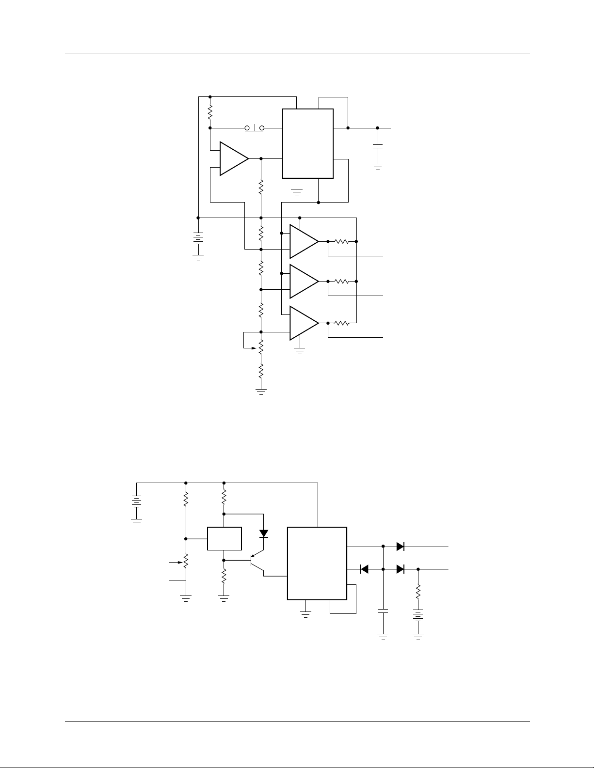
*Optional Latch off when drop out occurs. Adjust R3 for C2 Switching when V
**Outputs go low whenV
drops below designated thresholds.
in
Figure 12. Regulator with State-of-Charge Indicator
For values shown, Regulator shuts down when V
6V
+
Sealed
Lead-Acid
Battery
Source
≈ 400kΩ*
for 5.5V
*Sets disconnect Voltage
**Sets disconnect Hysteresis
< 5.5V and turns on again at 6.0V. Current drain in disconnected mode is ≈ 150 µA.
in
120kΩ
FB
LM385
1.5kΩ**
+
–
100kΩ
1N457
Figure 13. Low Battery Disconnect
3
is 6.0V.
in
SD
GND
8
+V
IN
RC2951
SENSE
V
TAP
1
V
OUT
2
7
FB
64
1µF
+
+
Main V+
Memory V+
20Ω
Ni-cad
Backup
Battery
2950-14
REV. 1.0.1 4/8/02 9
Page 10
RC2951 PRODUCT SPECIFICATION
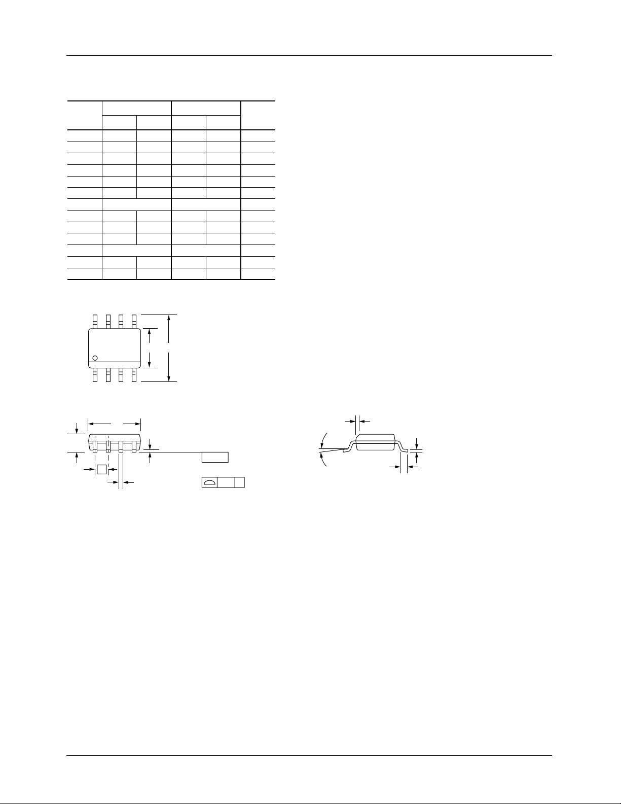
Mechanical Dimensions – 8 Lead SOIC
Symbol
A .053 .069 1.35 1.75
A1 .004 .010 0.10 0.25
B .013 0.33
C .008 .010 0.20 0.25
D .189 .197 4.80 5.00
E .150 .158 3.81 4.01
e
H
h
L .016 .050 0.40 1.27
N8 8
α
ccc .004 0.10——
85
14
Inches
Min. Max. Min. Max.
.020 0.51
.050 BSC 1.27 BSC
.228 .244 5.79 6.20
.010 .020 0.25 0.50
0° 8° 0° 8°
EH
Millimeters
Notes
5
2
2
3
6
Notes:
1.
Dimensioning and tolerancing per ANSI Y14.5M-1982.
2.
"D" and "E" do not include mold flash. Mold flash or
protrusions shall not exceed .010 inch (0.25mm).
3.
"L" is the length of terminal for soldering to a substrate.
4.
Terminal numbers are shown for reference only.
5.
"C" dimension does not include solder finish thickness.
6.
Symbol "N" is the maximum number of terminals.
D
A
e
B
A1
SEATING
PLANE
– C –
LEAD COPLANARITY
ccc C
α
h x 45°
C
L
10 REV. 1.0.1 4/8/02
Page 11

RC2951 PRODUCT SPECIFICATION
Ordering Information
Product Number Package
RC2951MT 8-pin SOIC in tape and reel
RC2951M33 8-pin SOIC
DISCLAIMER
FAIRCHILD SEMICONDUCTOR RESERVES THE RIGHT TO MAKE CHANGES WITHOUT FURTHER NOTICE TO
ANY PRODUCTS HEREIN TO IMPROVE RELIABILITY, FUNCTION OR DESIGN. FAIRCHILD DOES NOT ASSUME
ANY LIABILITY ARISING OUT OF THE APPLICATION OR USE OF ANY PRODUCT OR CIRCUIT DESCRIBED HEREIN;
NEITHER DOES IT CONVEY ANY LICENSE UNDER ITS PATENT RIGHTS, NOR THE RIGHTS OF OTHERS.
LIFE SUPPORT POLICY
FAIRCHILD’S PRODUCTS ARE NOT AUTHORIZED FOR USE AS CRITICAL COMPONENTS IN LIFE SUPPORT DEVICES
OR SYSTEMS WITHOUT THE EXPRESS WRITTEN APPROVAL OF THE PRESIDENT OF FAIRCHILD SEMICONDUCTOR
CORPORATION. As used herein:
1. Life support devices or systems are devices or systems
which, (a) are intended for surgical implant into the body,
or (b) support or sustain life, and (c) whose failure to
perform when properly used in accordance with
instructions for use provided in the labeling, can be
reasonably expected to result in a significant injury of the
user.
2. A critical component in any component of a life support
device or system whose failure to perform can be
reasonably expected to cause the failure of the life support
device or system, or to affect its safety or effectiveness.
www.fairchildsemi.com
4/8/02 0.0m 001
2001 Fairchild Semiconductor Corporation
Stock#DS30002951
 Loading...