Fairchild NC7WZ241 service manual

NC7WZ241
NC7WZ241 TinyLogic
March 2001
Revised January 2005
TinyLogic
General Description
The NC7WZ241 is a Dual Non-Inverting Buffer with
3-STATE outpu ts. The output enable circuitry is organized
as active LOW for one buffer and active HIGH for the other
buffer, thus facilitating transceiver operation.
The Ultra High Speed device is fabricated wit h advanced
CMOS technology to achieve superior switching performance with high output drive while maintaining low static
power dissipation over a br oad V
device is specified to o perate over the 1.65V to 5.5V V
operating range. Th e inputs and outputs are h igh imped-
ance when V
independent of V
ages above V
UHS Dual Buffer with 3-STATE Outputs
Features
■ Space saving US8 surface mount package
Pb-Free leadless package
3.3V V
CC
translation
2.6 ns Typ into 50 pF at 5V V
PD
operating range. The
CC
is 0V. Inputs tolerate voltages up to 5.5V
CC
operating range. Outp uts tolera te vol t-
CC
when in the 3-STATE condition.
CC
■ MicroPak
■ Ultra High Speed; t
■ High Output Drive; ±24 mA at 3V V
■ Broad VCC Operating Range: 1.65V to 5.5V
■ Matches the performance of LCX when operated at
CC
■ Power down high impedance inputs/outputs
■ Overvoltage tolerant inputs facilitate 5V to 3V
■ Outputs are overvoltage tolerant in 3-STATE mode
■ Patented noise/EMI reduction circuitry implemented
CC
CC
Ordering Code:
Product
Package Description Supplied AsOrder Package Code
Number Number Top Mark
NC7WZ241K8X MAB08A WZ41 8-Lead US8, JEDEC MO-187, Variation CA 3.1mm Wide 3k Units on Tape and Reel
NC7WZ241L8X MAC08A T7 Pb-Free 8-Lead MicroPak, 1.6 mm Wide 5k Units on Tape and Reel
Pb-Free pac k age per JEDEC J-STD-020B.
UHS Dual Buffer with 3-STATE Outputs
TinyLogic is a reg is t ered trademark of Fairc hild Semiconduct or Corporation.
MicroPak is a tradem ark of Fairchild Semiconductor Corporation.
© 2005 Fairchild Semiconductor Corporation DS500399 www.fairchildsemi.com

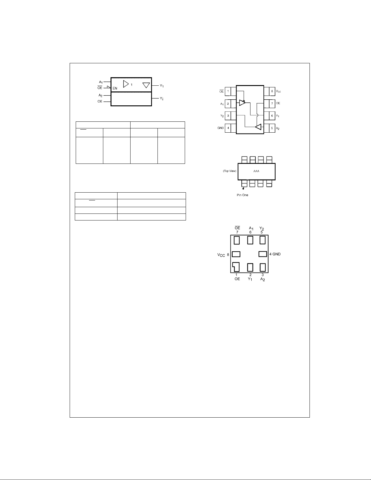
Logic Symbol
NC7WZ241
Function Table
Inputs Output
or OE
OE
LLLZ
LHHZ
HLZL
HHZH
H = HIGH Logic Level
L = LOW Logic Level
Z = 3-STATE
Pin Descriptions
Pin Names Description
OE
, OE Enable Inputs for 3-STATE Outputs
A
n
Y
n
Connection Diagrams
Pin Assignments f or US8
A
n
Y
1
Inputs
3-STATE Outputs
Y
2
Pin One Orientation Diagram
AAA represents Product Code Top Mark - see ordering cod e
Note: Orientation of Top Mark determines Pin One location. Read the top
product code mark lef t to right, Pin One is the lo w er left pin (see diagram ).
Pad Assignments for MicroPak
(Top View)
www.fairchildsemi.com 2
(Top Thru View)

Absolute Maximum Ratings(Note 1) Recommended Operating
Supply Voltage (VCC) −0.5V to +7.0V
DC Input Voltage (V
DC Output Voltage (V
DC Input Diode Current (I
@V
< 0V −50 mA
IN
DC Output Diode Current (I
< 0V −50 mA
@V
OUT
DC Output Source/Sink Current (I
DC V
/GND Current (ICC/I
CC
Storage Temperature Range (T
Junction Temperature under Bias (T
Junction Lead Temperature (T
(Soldering, 10 seconds)
Power Dissipation (P
) (Note 2) −0.5V to +7.0V
IN
) −0.5V to +7.0V
OUT
)
IK
)
OK
) ±50 mA
OUT
) ±100 mA
GND
) −65°C to +150°C
STG
) +150°C
J
)
L
+260°C
) @+85°C 250 mW
D
Conditions
Supply Voltage Operating (V
Supply Voltage Data Retention (V
Input Voltage (V
Output Voltage (V
Active State 0V to V
3-State 0V to 5.5V
Operating Temperature (T
Input Rise and Fall Time (t
V
= 1.8V, 0.15V, 2.5V ± 0.2V 0 ns/V to 20 ns/V
CC
= 3.8V ± 0.3V 0 ns/V to 10 ns/V
V
CC
V
= 5.0V ± 0.5V 0 ns/V to 5 ns/V
CC
Thermal Resistance (
Note 1: Absolute maximum ratings are DC values beyond which t he devi ce
may be damag ed or hav e it s usefu l li fe i mpa ired. Th e da tas heet sp ecific ations should be met, without exception, to ensure that the system design is
reliable over its power supply, temperature, and output/input loading variables. Fairchild does not recommend operation outside datasheet specifications.
Note 2: The input and output ne gat ive volt age ra ting s may be exc eeded is
the input and ou t put diode current ratings are observed.
Note 3: Unused inputs must be held HIGH or LOW. They may not float.
(Note 3)
) 1.65V to 5.5V
CC
) 1.5V to 5.5V
) 0V to 5.5V
IN
)
OUT
θ
JA
CC
) −40°C to +85°C
A
, tf)
r
)250°C/W
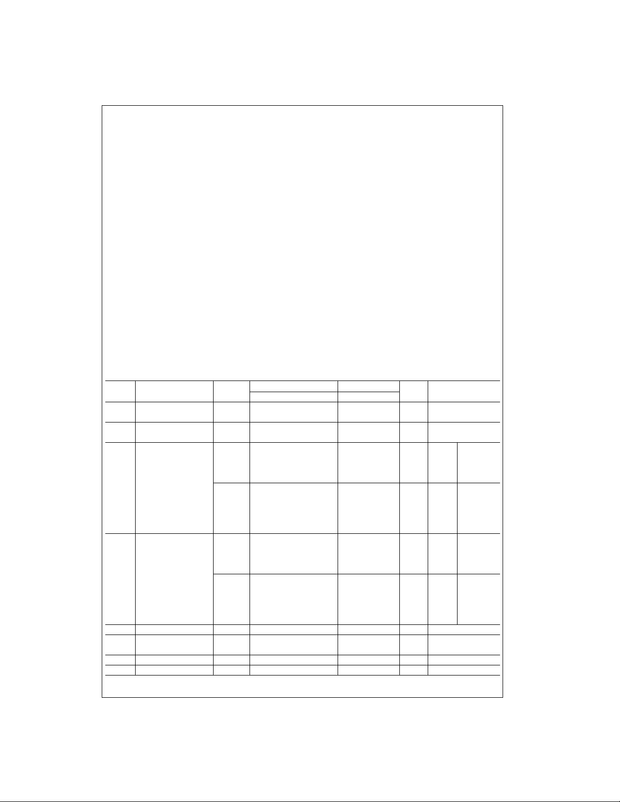
DC Electrical Characteristics
Symbol Parameter
V
HIGH Level Input Voltage 1.65 to 1.95 0.75 V
IH
V
LOW Level Input Voltage 1.65 to 1.95 0.25 V
IL
V
HIGH Level Output Voltage 1.65 1.55 1.65 1.55
OH
V
LOW Level Output Voltage 1.65 0.0 0.10 0.10
OL
I
Input Leakage Current 0 to 5.5 ±0.1 ±1 µAVIN = 5.5V, GND
IN
I
3-STATE Output Leakage 1.65 to 5.5 ±0.5 ±5 µAVIN = VIH or V
OZ
I
Power Off Leakage Current 0.0 1 10 µAVIN or V
OFF
I
Quiescent Supply Current 1.65 to 5.5 1 10 µAVIN = 5.5V, GND
CC
V
CC
(V) Min Typ Max Min Max
2.3 to 5.5 0.7 V
2.3 to 5.5 0.3 V
2.3 2.2 2.3 2.2 V
3.0 2.9 3.0 2.9 or V
4.5 4.4 4.5 4.4
1.65 1.29 1.52 1.29
2.3 1.9 2.15 1.9 V
3.0 2.4 2.80 2.4 or VILIOH = −16 mA
3.0 2.3 2.68 2.3 IOH = −24 mA
4.5 3.8 4.20 3.8 IOH = −32 mA
2.3 0.0 0.10 0.10 VIN = VIHIOL = 100 µA
3.0 0.0 0.10 0.10 or V
4.5 0.0 0.10 0.10
1.65 0.08 0.24 0.24
2.3 0.10 0.3 0.3 VIN = VIHIOL = 8 mA
3.0 0.15 0.4 0.4 or VILIOL = 16 mA
3.0 0.22 0.55 0.55 IOL = 24 mA
4.5 0.22 0.55 0.55 IOL = 32 mA
TA = +25°CT
CC
CC
= −40°C to +85°C
A
0.75 V
0.7 V
CC
CC
Unit Conditions
CC
CC
0.25 V
0.3 V
V
CC
V
CC
V
V
V
V
0 ≤ V
= VIHIOH = −100 µA
IN
IL
I
= −4 mA
OH
= VIHIOH = −8 mA
IN
IL
IOL = 4 mA
IL
≤ 5.5V
OUT
= 5.5V
OUT
NC7WZ241
CC
3 www.fairchildsemi.com
 Loading...