Fairchild NC7WZ240 service manual

NC7WZ240
NC7WZ240 TinyLogic
March 2001
Revised January 2005
TinyLogic
UHS Dual Inverting Buffer
with 3-STATE Outputs
General Description
The NC7WZ240 is a Dual Inverting Buffer with inde pendent active LOW enables for the 3-STATE outputs. The
Ultra High Speed device is fabricated with advanced
CMOS technology to achieve superior switching performance with high output drive while maintaining low static
power dissipation over a br oad V
device is specified to o perate over the 1.65V to 5.5V V
operating range. Th e inputs and outputs are h igh imped-
ance when V
independent of V
ages above V
is 0V. Inputs tolerate voltages up to 5.5V
CC
operating range. Outp uts tolera te vol t-
CC
when in the 3-STATE condition.
CC
operating range. The
CC
Ordering Code:
Product
Number Number Top Mark
NC7WZ240K8X MAB08A WZ40 8-Lead US8, JEDEC MO-187, Variation CA 3.1mm Wide 3k Units on Tape and Reel
NC7WZ240L8X MAC08A U7 Pb-Free 8-Lead MicroPak, 1.6 mm Wide 5k Units on Tape and Reel
Pb-Free pac k age per JEDEC J-STD-020 B.
Features
■ Space saving US8 surface mount package
■ MicroPak
■ Ultra High Speed; t
■ High Output Drive; ±24 mA at 3V V
■ Broad VCC Operating Range: 1.65V to 5.5V
CC
■ Matches the performance of LCX when operated at
■ Power down high impedance inputs/outputs
■ Overvoltage tolerant inputs facilitate 5V to 3V translation
■ Outputs are overvoltage tolerant in 3-STATE mode
■ Proprietary noise/EMI reduction circuitry implemented
Package Description Supplied AsOrder Package Code
Pb-Free leadless package
3.3V V
CC
2.3 ns typ into 50 pF at 5V V
PD
CC
CC
UHS Dual Inverting Buffer with 3-STATE Outputs
TinyLogic is a registered trademark of Fairchild Semiconductor Co rporation.
MicroPak is a tradem ark of Fairchild Semiconductor Corporation.
© 2005 Fairchild Semiconductor Corporation DS500398 www.fairchildsemi.com

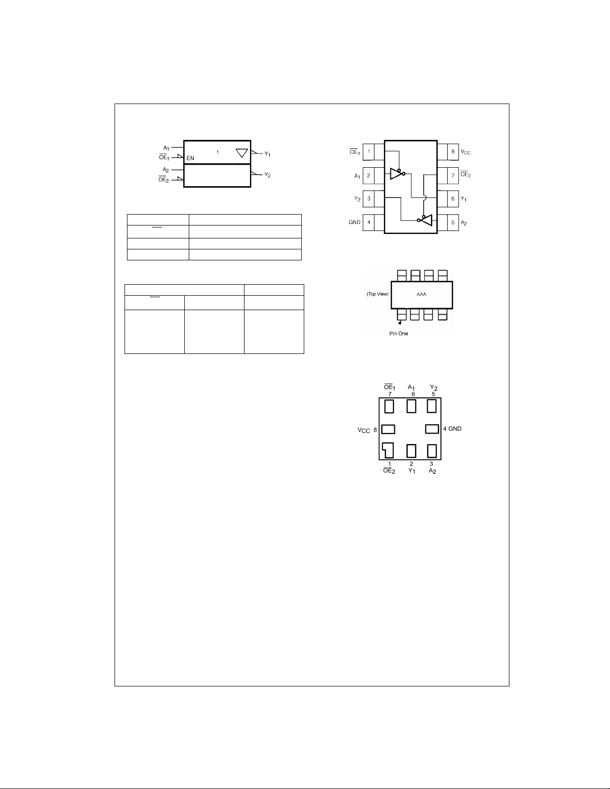
Logic Symbol
Connection Diagrams
IEEE/IEC
NC7WZ240
Pin Descriptions
Pin Names Description
OE
A
n
Y
n
Enable Inputs for 3-STATE Outputs
n
3-STATE Outputs
Inputs
Function Table
Inputs Output
OE
LLH
LHL
HLZ
HHZ
H = HIGH Logic Level L = LOW Logic Level Z = 3-STATE
A
n
Pin Assignments f or US8
(Top View)
Pin One Orientation Diagram
Y
n
AAA represents Product Code Top Mark - see ordering cod e
Note: Orientation of Top Mark determines Pin One location. Read the top
product code mark lef t to right, Pin One is the lo w er left pin (see diagram ).
Pad Assignment for MicroPak
www.fairchildsemi.com 2
(Top Through View)

Absolute Maximum Ratings(Note 1) Recommended Operating
Supply Voltage (VCC) −0.5V to +7.0V
DC Input Voltage (V
DC Output Voltage (V
DC Input Diode Current (I
@V
< 0V −50 mA
IN
DC Output Diode Current (I
< 0V −50 mA
@V
OUT
DC Output Source/Sink Current (I
DC V
/Ground Cu rrent (ICC/I
CC
Storage Temperature Range (T
Junction Lead Temperature under Bias (T
Junction Lead Temperature (T
(Soldering, 10 seconds)
Power Dissipation (P
) (Note 2) −0.5V to +7.0V
IN
) −0.5V to +7.0V
OUT
)
IK
)
OK
) ± 50 mA
OUT
) ± 100 mA
GND
) −65°C to +150°C
L
STG
)
) +150°C
J
+260°C
) @ +85°C250 mW
D
Conditions
Supply Voltage Operating (V
Supply Voltage Data Retention (V
Input Voltage (V
Output Voltage (V
Active State 0V to V
3-STATE 0V to 5.5V
Operating Temperature (T
Input Rise and Fall Time (t
V
@ 1.8V, 0.15V, 2.5V ± 0.2V 0 ns/V to 20 ns/V
CC
@ 3.3V ± 0.3V 0 ns/V to 10 ns/V
V
CC
V
@ 5.0V ± 0.5V 0 ns/V to 5 ns/V
CC
Thermal Resistance (
Note 1: Absolute maximum ratings are DC values beyond which t he devi ce
may be damag ed or hav e it s usefu l li fe i mpa ired. Th e da tas heet sp ecific ations should be met, without exception, to ensure that the system design is
reliable over its power supply, temperature, and output/input loading variables. Fairchild does not recommend operation outside datasheet specifications.
Note 2: The input and output negative voltage ratings may be exceeded if
the input and ou t put diode current ra t ings are observed.
Note 3: Unused inputs must be held HIGH or LOW. They may not float.
(Note 3)
) 1.65V to 5.5V
CC
) 1.5V to 5.5V
) 0V to 5.5V
IN
)
OUT
θ
JA
CC
) −40°C to +85°C
A
, tf)
r
)250°C/W
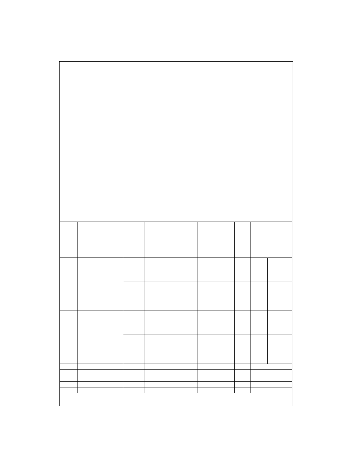
DC Electrical Characteristics
Symbol Parameter
V
HIGH Level Input Voltage 1.65 to 1.95 0.75 V
IH
V
LOW Level Input Voltage 1.65 to 1.95 0.25 V
IL
V
HIGH Level Output Voltage 1.65 1.55 1.65 1.55
OH
V
LOW Level Output Voltage 1.65 0.0 0.10 0.10
OL
I
Input Leakage Current 0 to 5.5 ±0.1 ±1 µAVIN = 5.5V, GND
IN
I
3-STATE Output Leakage 1.65 to 5.5 ±0.5 ±5 µAVIN = VIH or V
OZ
I
Power Off Leakage Current 0.0 1 10 µAVIN or V
OFF
I
Quiescent Supply Current 1.65 to 5.5 1 10 µAVIN = 5.5V, GND
CC
V
CC
(V) Min Typ Max Min Max
2.3 to 5.5 0.7 V
2.3 to 5.5 0.3 V
2.3 2.2 2.3 2.2 V
3.0 2.9 3.0 2.9 or V
4.5 4.4 4.5 4.4
1.65 1.29 1.52 1.29
2.3 1.9 2.15 1.9 V
3.0 2.4 2.80 2.4 or VILIOH = −16 mA
3.0 2.3 2.68 2.3 IOH = −24 mA
4.5 3.8 4.20 3.8 IOH = −32 mA
2.3 0.0 0.10 0.10 VIN = VIHIOL = 100 µA
3.0 0.0 0.10 0.10 or V
4.5 0.0 0.10 0.10
1.65 0.08 0.24 0.24
2.3 0.10 0.3 0.3 IOL = 8 mA
3.0 0.15 0.4 0.4 IOL = 16 mA
3.0 0.22 0.55 0.55 IOL = 24 mA
4.5 0.22 0.55 0.55 IOL = 32 mA
TA = +25°CT
CC
CC
= −40°C to +85°C
A
0.75 V
0.7 V
CC
CC
Units Conditions
CC
CC
0.25 V
0.3 V
V
CC
V
CC
V
V
V
V
= VIHIOH = −100 µA
IN
IL
I
= −4 mA
OH
= VIHIOH = −8 mA
IN
IL
IOL = 4 mA
OUT
≤ 5.5V
OUT
IL
= 5.5V
0 ≤ V
NC7WZ240
CC
3 www.fairchildsemi.com
 Loading...