

®
NC7WZ07
TinyLogic
®
UHS Dual Buffer (Open Drain Outputs)
NC7WZ07 — TinyLogic
January 2011
UHS Dual Buffer (Open Drain Outputs)
Features
Ultra-High Speed: t
High I
Broad V
Output Drive: ±24mA at 3V VCC
OL
Operating Range: 1.65V to 5.50V
CC
2.3ns (Typical)
PZL
Power Down High Impedance Inputs/Outputs
Over-Voltage Tolerance Inputs Facilitate 5V to 3V
Translation
Proprietary Noise/EMI Reduction Circuitry
Ultra-Small MicroPak™ Packages
Description
The NC7WZ07 is a dual buffer with open drain outputs
from Fairchild’s Ultra-High Speed (UHS) series of
TinyLogic®. The device is fabricated with advanced
CMOS technology to achieve ultra-high speed with high
output drive while maintaining low static power
dissipation over a broad V
device is specified to operate over a very broad V
operating range. The device is specified to operate over
the 1.65V to 5.5V V
high impedance when V
up to 7V independent of V
range. The inputs and outputs are
CC
CC
operating range. The
CC
is 0V. Inputs tolerate voltages
operating voltage.
CC
Ordering Information
Part Number Top Mark Package Packing Method
NC7WZ07P6X Z07 6-Lead SC70, EIAJ SC88 1.25mm Wide 3000 Units on Tape & Reel
NC7WZ07L6X D3 6-Lead MicroPak™, 1.00mm Wide 5000 Units on Tape & Reel
NC7WZ07FHX D3 6-Lead, MicroPak2™, 1x1mm Body, .35mm Pitch 5000 Units on Tape & Reel
CC
© 2000 Fairchild Semiconductor Corporation www.fairchildsemi.com
NC7WZ07 • Rev. 1.0.6
®
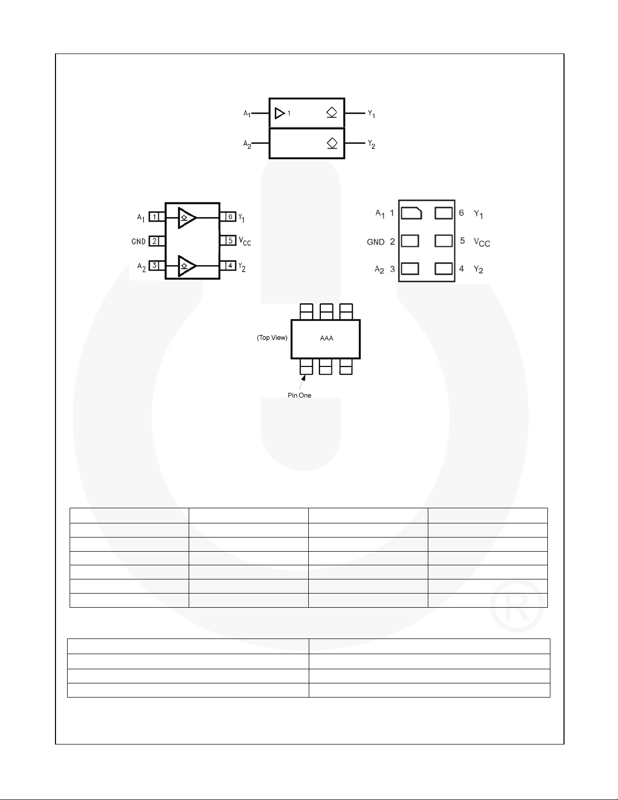
Connection Diagrams
NC7WZ07 — TinyLogic
IEEE/IEC
Figure 1. Logic Symbol
Pin Configurations
Figure 2. SC70 (Top View) Figure 3. MicroPak™ (Top Through View)
Figure 4. Pin 1 Orientation
Notes:
1. AAA represents product code top mark (see Ordering Information).
2. Orientation of top mark determines pin one location.
3. Reading the top mark left to right, pin one is the lower left pin.
UHS Dual Buffer (Open Drain Outputs)
Pin Definitions
Pin # SC70 Pin # MicroPak™ Name Description
1 1 A1 Input
2 2 GND Ground
3 3 A2 Input
4 4 Y2 Output
5 5 VCC Supply Voltage
6 6 Y1 Output
Function Table
Y= A
Inputs Output
A Y
L L
H H*
H = HIGH Logic Level
L = LOW Logic Level
H* = High Impedance Output State, Open Drain
© 2000 Fairchild Semiconductor Corporation www.fairchildsemi.com
NC7WZ07 • Rev. 1.0.6 2
®
NC7WZ07 — TinyLogic
Absolute Maximum Ratings
Stresses exceeding the absolute maximum ratings may damage the device. The device may not function or be
operable above the recommended operating conditions and stressing the parts to these levels is not recommended.
In addition, extended exposure to stresses above the recommended operating conditions may affect device reliability.
The absolute maximum ratings are stress ratings only.
Symbol Parameter Min. Max. Unit
VCC Supply Voltage -0.5 7.0 V
VIN DC Input Voltage -0.5 7.0 V
V
DC Output Voltage -0.5 7.0 V
OUT
IIK DC Input Diode Current VIN < -0.5V -50 mA
IOK DC Output Diode Current V
I
DC Output Current ±50 mA
OUT
ICC or I
DC VCC or Ground Current ±100 mA
GND
T
Storage Temperature Range -65 +150 °C
STG
< -0.5V -50 mA
OUT
TJ Junction Temperature Under Bias +150 °C
TL Junction Lead Temperature (Soldering, 10 Seconds) +260 °C
SC70-6 180
PD Power Dissipation at +85°C
MicroPak2™-6 120
ESD
Human Body Model, JEDEC:JESD22-A114 4000
Charge Device Model, JEDEC:JESD22-C101 2000
mW MicroPak™-6 130
V
UHS Dual Buffer (Open Drain Outputs)
Recommended Operating Conditions
The Recommended Operating Conditions table defines the conditions for actual device operation. Recommended
operating conditions are specified to ensure optimal performance to the datasheet specifications. Fairchild does not
recommend exceeding them or designing to Absolute Maximum Ratings.
Symbol Parameter Conditions Min. Max. Unit
VCC
VIN Input Voltage 0 5.5 V
V
OUT
tr, tf Input Rise and Fall Times
TA Operating Temperature -40 +85 °C
JA
Note:
4. Unused inputs must be held HIGH or LOW. They may not float.
Supply Voltage Operating 1.65 5.50
Supply Voltage Data Retention 1.5 5.5
V
Output Voltage 0 5.5 V
at 1.8V, ±0.15V,
V
CC
2.5V ± 0.2V
VCC at 3.3V ± 0.3V 0 10
0 20
ns/V
VCC at 5.0V ± 0.5V 0 5
SC70-6 425
Thermal Resistance
MicroPak™-6 500
°C/W
MicroPak2™-6 560
© 2000 Fairchild Semiconductor Corporation www.fairchildsemi.com
NC7WZ07 • Rev. 1.0.6 3

®
DC Electrical Characteristics
Symbol Parameter VCC Conditions
VIH
VIL
HIGH Level Input
Voltage
LOW Level Input
Voltage
1.65 to 1.95
2.30 to 5.50
1.65 to 1.95
2.30 to 5.50
HIGH Level
I
LKG
Output Leakage
1.65 to 5.50
Current
1.65
1.80 0.00 0.10 0.10
2.30 0.00 0.10 0.10
3.00 0.00 0.10 0.10
VOL
LOW Level
Output Voltage
4.50 0.00 0.10 0.10
1.65 IOL=4mA 0.80 0.24 0.24
2.30 IOL=8mA 0.10 0.30 0.30
3.00 IOL=16mA 0.16 0.40 0.40
3.00 IOL=24mA 0.24 0.55 0.55
4.50 IOL=32mA 0.25 0.55 0.55
Input Leakage
I
ICC
IIN
OFF
Current
Power Off
Leakage Current
Quiescent Supply
Current
0 to 5.5
0 V
1.65 to 5.50 VIN=5.5V, GND 1 10 µA
V
IN=VIH
V
OUT=VCC
V
IN=VIL
0 V
or V
IN
,
or GND
, IOL=100µA
5.5V
IN
=5.5V 1 10 µA
OUT
=+25°C TA=-40 to +85°C
T
A
Units
Min. Typ. Max. Min. Max.
0.75VCC
0.75V
CC
0.70VCC 0.70VCC
0.25V
0.30V
CC
CC
0.25VCC
0.30VCC
±5 ±10 µA
0.00 0.10 0.00
±0.1 ±1.0 µA
V
V
V
NC7WZ07 — TinyLogic
UHS Dual Buffer (Open Drain Outputs)
© 2000 Fairchild Semiconductor Corporation www.fairchildsemi.com
NC7WZ07 • Rev. 1.0.6 4

®
AC Electrical Characteristics
=-40 to
T
=+25°C
T
Symbol Parameter VCC Conditions
A
Min. Typ. Max. Min. Max.
1.65
C
=50pF,
L
RU=500
RD=500
=2 x VCC
V
I
=50pF,
C
L
RU=500
RD=500
=2 x VCC
V
I
t
, t
Propagation Delay
PZL
PLZ
1.80 1.8 5.5 9.5 1.8 10.5
2.50 ± 0.20 1.2 3.7 5.8 1.2 6.4
3.30 ± 0.30 0.8 2.9 4.4 0.8 4.8
5.00 ± 0.50 0.5 2.3 3.5 0.5 3.9
1.65
1.80 1.8 4.3 9.5 1.8 10.5
2.50 ± 0.20 1.2 2.8 5.8 1.2 6.4
3.30 ± 0.30 0.8 2.1 4.4 0.8 4.8
5.00 ± 0.50 0.5 1.4 3.5 0.5 3.9
CIN Input Capacitance 0 2.5 pF
C
Output Capacitance 0 4.0
OUT
CPD
Power Dissipation
Capacitance
(5)
3.30
5.00 4
1.8 6.6 11.5 1.8 12.6
1.8 5.5 11.5 1.8 12.6
3
Note:
5. CPD is defined as the value of the internal equivalent capacitance which is derived from dynamic operating
current consumption (I
operating current by the expression: I
) at no output loading and operating at 50% duty cycle. CPD is related to I
CCD
=(CPD)(VCC)(fIN)+(ICCstatic).
CCD
A
+85°C
Units Figure
ns
Figure 5
Figure 6
pF Figure 7
dynamic
CCD
NC7WZ07 — TinyLogic
UHS Dual Buffer (Open Drain Outputs)
Notes:
6. CL includes load and stray capacitance.
7. Input PRR = 1.0MHz, t
= 500ns.
W
Figure 5. AC Test Circuit Figure 6. AC Waveforms
Note:
8. Input=AC Waveform; tr=tf=1.8ns.
9. PRR=Variable; Duty Cycle=50%.
Figure 7. I
© 2000 Fairchild Semiconductor Corporation www.fairchildsemi.com
NC7WZ07 • Rev. 1.0.6 5
Test Circuit
CCD

®
Physical Dimensions
NC7WZ07 — TinyLogic
SYMM
C
L
±0.20
2.00
6
A
4
B
0.65
0.50 MIN
PIN ONE
(0.25)
GAGE
PLANE
0.20
1.00
0.80
C
1.25
±0.10
1.90
UHS Dual Buffer (Open Drain Outputs)
1
0.65
1.30
3
0.10
0.00
SEATING
PLANE
0.30
0.15
0.10 AB
1.10
0.80
(R0.10)
0.40 MIN
1.30
LAND PATTERN RECOMMENDATION
SEE DETAIL A
0.10
C
2.10±0.30
NOTES: UNLESS OTHERWISE SPECIFIED
A) THIS PACKAGE CONFORMS TO EIAJ
SC-88, 1996.
B) ALL DIMENSIONS ARE IN MILLIMETERS.
C) DIMENSIONS DO NOT INCLUDE BURRS
0.25
OR MOLD FLASH.
0.10
D) DRAWING FILENAME: MKT-MAA06AREV6
0.46
0.26
DETAIL A
SCALE: 60X
30°
0°
Figure 8. 6-Lead, SC70, EIAJ SC88, 1.25mm Wide
Package drawings are provided as a service to customers considering Fairchild components. Drawings may change in any manner
without notice. Please note the revision and/or date on the drawing and contact a Fairchild Semiconductor representative to verify or
obtain the most recent revision. Package specifications do not expand the terms of Fairchild’s worldwide terms and conditions, specifically the
warranty therein, which covers Fairchild products.
Always visit Fairchild Semiconductor’s online packaging area for the most recent package drawings:
http://www.fairchildsemi.com/packaging/
.
Tape and Reel Specification
Please visit Fairchild Semiconductor’s online packaging area for the most recent tape and reel specifications:
http://www.fairchildsemi.com/products/analog/pdf/sc70-6_tr.pdf
Package Designator Tape Section Cavity Number Cavity Status Cover Type Status
Leader (Start End) 125 (Typical) Empty Sealed
P6X
© 2000 Fairchild Semiconductor Corporation www.fairchildsemi.com
NC7WZ07 • Rev. 1.0.6 6
Carrier 3000 Filled Sealed
Trailer (Hub End) 75 (Typical) Empty Sealed
.

®
Physical Dimensions
2X
1.45
2X
NC7WZ07 — TinyLogic
B0.05 C
(1)
0.05 C
(0.254)
PIN 1 IDENTIFIER
5
0.05 C
DETAIL A
(0.05)
6X
Notes:
1. CONFORMS TO JEDEC STANDARD M0-252 VARIATION UAAD
2. DIMENSIONS ARE IN MILLIMETERS
3. DRAWING CONFORMS TO ASME Y14.5M-1994
4. FILENAME AND REVISION: MAC06AREV4
5. PIN ONE IDENTIFIER IS 2X LENGTH OF ANY
OTHER LINE IN THE MARK CODE LAYOUT.
TOP VIEW
0.55MAX
C
1.0
0.5
BOTTOM VIEW
1.00
A
0.05
0.00
0.05 C
0.25
6X
0.15
0.10 CBA
0.05
0.35
5X
0.25
0.40
5X
0.30
(0.13)
4X
C
(0.49)
5X
(0.52)
1X
PIN 1
0.075 X 45
CHAMFER
(0.30)
6X
RECOMMENED
LAND PATTERN
0.10
6X
0.00
DETAIL A
PIN 1 TERMINAL
0.40
0.30
(0.75)
0.45
0.35
Figure 9. 6-Lead, MicroPak™, 1.0mm Wide
Package drawings are provided as a service to customers considering Fairchild components. Drawings may change in any manner
without notice. Please note the revision and/or date on the drawing and contact a Fairchild Semiconductor representative to verify or
obtain the most recent revision. Package specifications do not expand the terms of Fairchild’s worldwide terms and conditions, specifically the
warranty therein, which covers Fairchild products.
Always visit Fairchild Semiconductor’s online packaging area for the most recent package drawings:
http://www.fairchildsemi.com/packaging/
.
UHS Dual Buffer (Open Drain Outputs)
Tape and Reel Specification
Please visit Fairchild Semiconductor’s online packaging area for the most recent tape and reel specifications:
http://www.fairchildsemi.com/products/logic/pdf/micropak_tr.pdf
Package Designator Tape Section Cavity Number Cavity Status Cover Type Status
Leader (Start End) 125 (Typical) Empty Sealed
L6X
© 2000 Fairchild Semiconductor Corporation www.fairchildsemi.com
NC7WZ07 • Rev. 1.0.6 7
Carrier 5000 Filled Sealed
Trailer (Hub End) 75 (Typical) Empty Sealed
.

®
Physical Dimensions
0.05
C
2X
1.00
NC7WZ07 — TinyLogic
0.89
B
A
5X 0.40
0.35
PIN 1
MIN 250uM
TOP VIEW
C
SIDE VIEW
(0.08) 4X
DETAIL A
0.35
5X
0.25
NOTES:
A. COMPLIES TO JEDEC MO-252 STANDARD
B. DIMENSIONS ARE IN MILLIMETERS.
C. DIMENSIONS AND TOLERANCES PER ASME Y14.5M, 1994
D. LANDPATTERN RECOMMENDATION IS BASED ON FSC
DESIGN.
E. DRAWING FILENAME AND REVISION: MGF06AREV3
123
654
0.35
BOTTOM VIEW
0.55MAX
0.09
0.19
0.60
(0.08)
4X
1.00
2X
0.05
6X
0.10 CBA
.05
0.05
C
C
1X 0.45
C
RECOMMENDED LAND PATTERN
FOR SPACE CONSTRAINED PCB
5X
0.52
0.57
1X
ALTERNATIVE LAND PATTERN
FOR UNIVERSAL APPLICATION
(0.05) 6X
0.075X45°
CHAMFER
DETAIL A
PIN 1 LEAD SCALE: 2X
6X 0.19
0.90
0.35
0.20 6X
0.66
0.73
0.40
0.30
Figure 10. 6-Lead, MicroPak2™, 1x1mm Body, .35mm Pitch
Package drawings are provided as a service to customers considering Fairchild components. Drawings may change in any manner
without notice. Please note the revision and/or date on the drawing and contact a Fairchild Semiconductor representative to verify or
obtain the most recent revision. Package specifications do not expand the terms of Fairchild’s worldwide terms and conditions, specifically the
warranty therein, which covers Fairchild products.
Always visit Fairchild Semiconductor’s online packaging area for the most recent package drawings:
http://www.fairchildsemi.com/packaging/
.
UHS Dual Buffer (Open Drain Outputs)
Tape and Reel Specification
Please visit Fairchild Semiconductor’s online packaging area for the most recent tape and reel specifications:
http://www.fairchildsemi.com/packaging/MicroPAK2_6L_tr.pdf
Package Designator Tape Section Cavity Number Cavity Status Cover Type Status
Leader (Start End) 125 (Typical) Empty Sealed
FHX
© 2000 Fairchild Semiconductor Corporation www.fairchildsemi.com
NC7WZ07 • Rev. 1.0.6 8
Carrier 5000 Filled Sealed
Trailer (Hub End) 75 (Typical) Empty Sealed
.

®
NC7WZ07 — TinyLogic
UHS Dual Buffer (Open Drain Outputs)
© 2000 Fairchild Semiconductor Corporation www.fairchildsemi.com
NC7WZ07 • Rev. 1.0.6 9
 Loading...