

Fairchild NC7WV14 service manual
NC7WV14 — TinyLogic
June 2008
NC7WV14
TinyLogic
®
ULP-A Dual Inverter with Schmitt Trigger Input
Features
■
0.9V to 3.6V V
■
3.6V overvoltage tolerant I/O’s at V
3.6V
■
Extremely High Speed t
– 1.5ns typ. for 2.7V to 3.6V V
– 1.8ns typ. for 2.3V to 2.7V V
– 2.0ns typ. for 1.65V to 1.95V V
– 3.2ns typ. for 1.4V to 1.6V V
– 5.9ns typ. for 1.1V to 1.3V V
– 12.0ns typ. for 0.9V V
■
Power-Off high impedance inputs and outputs
■
High Static Drive (I
– ±24mA @ 3.00V V
– ±18mA @ 2.30V V
– ±6mA @ 1.65V V
– ±4mA @ 1.4V V
– ±2mA @ 1.1V V
– ±0.1mA @ 0.9V V
Uses patented Quiet Series™ noise/EMI reduction
■
circuitry
■
Ultra small MicroPak™ package
Ultra low dynamic power
■
supply operation
CC
:
PD
CC
/I
):
OH
OL
CC
CC
CC
CC
CC
CC
CC
CC
CC
CC
CC
CC
from 0.9V to
General Description
The NC7WV14 is a dual inverter with Schmitt trigger
from Fairchild’s Ultra Low Power-A (ULP-A) Series
of TinyLogic
require extreme high speed, high drive and low power.
This product is designed for a wide low voltage operating
range (0.9V to 3.6V V
more drive and speed than the TinyLogic ULP series, but
still offer best in class low power operation.
The NC7WV14 is uniquely designed for optimized power
and speed, and is fabricated with an advanced CMOS
technology to achieve high-speed operation while maintaining low CMOS power dissipation.
. ULP-A is ideal for applications that
) and applications that require
CC
®
ULP-A Dual Inverter with Schmitt Trigger Input
Ordering Information
Order
Number
NC7WV14P6X MAA06A V14 6-Lead SC70, EIAJ SC88,
NC7WV14L6X MAC06A BD 6-Lead MicroPak, 1.0mm Wide 5k Units on Tape and Reel
All packages are lead free per JEDEC: J-STD-020B standard.
Battery Life vs. V
700
600
Battery Life
(Days)
©2003 Fairchild Semiconductor Corporation www.fairchildsemi.com
NC7WV14 Rev. 1.0.0
500
400
300
200
100
0
ULP-A (SV)
ULP (SP)
0.9 1.2
Package
Number
Supply Voltage
CC
1.5 1.8 2.5 3.3 5.0
Supply Voltage
V
CC
Package Code
Top Mark Package Description Supplied As
UHS (SZ)
3k Units on Tape and Reel
1.25mm Wide
TinyLogic ULP and ULP-A with up to 50% less power consumption can
extend your battery life significantly.
Battery Life = (V
Where, P
Assumes ideal 3.6V Lithium Ion battery with current rating of 900mAH
and derated 90% and device frequency at 10MHz, with CL = 15pF load.
device
battery
= (I
x I
battery
x VCC) + (C
CC
x 0.9) / (P
+ CL) x V
PD
device
) / 24hrs/day
2
x f
CC
Y =
H =
NC7WV14 — TinyLogic
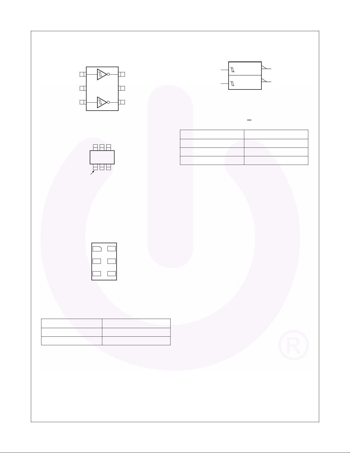
Connection Diagrams
Pin Assignment for SC70
1 6
A
1
2 5
GND
3 4
A
2
(Top View)
Pin One Orientation Diagram
(Top View)
Pin One
AAA represents Product Code Top Mark – see ordering code
Note: Orientation of top mark determines pin one location.
Read the top product code mark left to right. Pin one is the
lower left pin (see diagram).
AAA
Y
1
V
CC
Y
2
Logic Symbol
A
1
A
2
Function Table
Input Output
AY
LH
HL
HIGH Logic Level
L = LOW Logic Level
IEEE/IEC
1
A
Y
1
Y
2
®
ULP-A Dual Inverter with Schmitt Trigger Input
Pad Assignments for MicroPak
A
1
1
GND
2
A
3
2
(Top Through View)
Pin Description
Pin Names Description
A
, A
1
2
Y
, Y
1
2
Y
6
1
V
5
CC
Y
4
2
Data Inputs
Output
©2003 Fairchild Semiconductor Corporation www.fairchildsemi.com
NC7WV14 Rev. 1.0.0 2
=
<
<
>
=
=
=
=
=
=
=
NC7WV14 — TinyLogic
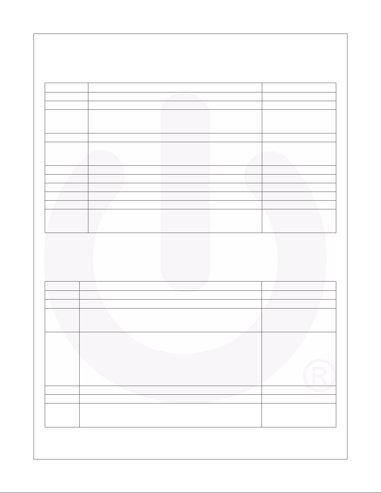
Absolute Maximum Ratings
Stresses exceeding the absolute maximum ratings may damage the device. The device may not function or be
operable above the recommended operating conditions and stressing the parts to these levels is not recommended.
In addition, extended exposure to stresses above the recommended operating conditions may affect device reliability.
The absolute maximum ratings are stress ratings only.
Symbol Parameter Rating
V
CC
V
IN
V
OUT
I
IK
I
OK
I
/
I
OH
OL
I
or Ground DC V
CC
T
STG
T
J
T
L
P
D
Supply Voltage –0.5V to +4.6V
DC Input Voltage –0.5V to +4.6V
DC Output Voltage
HIGH or LOW State
V
0V
CC
DC Input Diode Current @ V
(1)
–0.5V to V
–0.5V to +4.6V
0V –50mA
IN
CC
+0.5V
DC Output Diode Current
V
V
OUT
OUT
0V
V
CC
–50mA
+50mA
DC Output Source/Sink Current ±50mA
or Ground Current per Supply Pin ±50mA
CC
Storage Temperature Range –65°C to +150°C
Junction Temperature Under Bias 150°C
Junction Lead Temperature (Soldering, 10 seconds) 260°C
Power Dissipation @ +85°C
SC70-6
Micropak-6
185mW
210mW
®
ULP-A Dual Inverter with Schmitt Trigger Input
∆
∆ V
Recommended Operating Conditions
(2)
The Recommended Operating Conditions table defines the conditions for actual device operation. Recommended
operating conditions are specified to ensure optimal performance to the datasheet specifications. Fairchild does not
recommend exceeding them or designing to absolute maximum ratings.
Symbol Parameter Rating
V
CC
V
IN
V
OUT
I
/
OH
T
A
t
/
θ
JA
Supply Voltage 0.9V to 3.6V
Input Voltage 0V to 3.6V
Output Voltage
HIGH or LOW State
V
0V
CC
I
Output Current in I
OL
V
3.0V to 3.6V
CC
V
2.3V to 2.7V
CC
V
1.65V to 1.95V
CC
V
1.4V to 1.6V
CC
V
1.1V to 1.3V
CC
V
0.9V
CC
OH
/
I
OL
Free Air Operating Temperature –40°C to +85°C
Minimum Input Edge Rate @ V
= 0.8V to 2.0V, V
IN
= 3.0V 10ns/V
CC
Thermal Resistance
SC70-6
Micropak-6
0V to V
CC
0V to 3.6V
±24mA
±18mA
±6mA
±4mA
±2mA
±0.1mA
350°C/W
310°C/W
Notes:
1. I
Absolute Maximum Rating must be observed.
O
2. Unused inputs must be held HIGH or LOW. They may not float.
©2003 Fairchild Semiconductor Corporation www.fairchildsemi.com
NC7WV14 Rev. 1.0.0 3
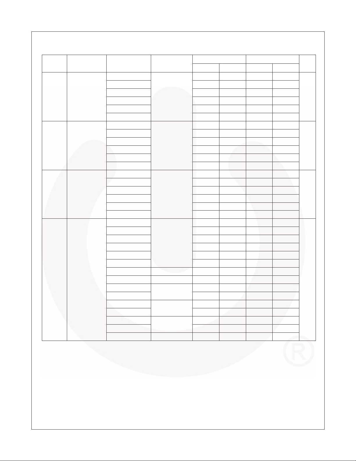
DC Electrical Characteristics
Symbol Parameter V
V
Positive
P
Threshold
Voltage
V
Negative
N
Threshold
Voltage
V
Hysteresis
H
Voltage
V
OH
HIGH Level
Output Voltage
1.10 ≤ VCC ≤ 1.30 VCC – 0.1 VCC – 0.1
1.40 ≤ VCC ≤ 1.60 VCC – 0.2 VCC – 0.2
1.65 ≤ VCC ≤ 1.95 VCC – 0.2 VCC – 0.2
2.30 ≤ VCC < 2.70 VCC – 0.2 VCC – 0.2
2.70 ≤ VCC ≤ 3.60 VCC – 0.2 VCC – 0.2
1.10 ≤ VCC ≤ 1.30 IOH = –2mA 0.75 x V
1.40 ≤ VCC ≤ 1.60 IOH = –4mA 0.75 x V
1.65 ≤ VCC ≤ 1.95 IOH = –6mA 1.25 1.25
2.30 ≤ V
2.30 ≤ VCC < 2.70 IOH = –12mA 1.8 1.8
2.70 ≤ VCC ≤ 3.60 2.2 2.2
2.30 ≤ VCC < 2.70 IOH = –18mA 1.7 1.7
2.70 ≤ VCC ≤ 3.60 2.4 2.4
2.70 ≤ VCC ≤ 3.60 IOH = –24mA 2.2 2.2
(V) Conditions
CC
0.90 0.3 0.7 0.3 0.7 V
1.10 0.4 1.0 0.4 1.0
1.40 0.5 1.4 0.5 1.4
1.65 0.7 1.5 0.7 1.5
2.30 1.0 1.8 1.0 1.8
2.70 1.3 2.2 1.3 2.2
0.90 0.10 0.6 0.10 0.6 V
1.10 0.15 0.7 0.15 0.7
1.40 0.20 0.8 0.20 0.8
1.65 0.25 0.9 0.25 0.9
2.30 0.4 1.15 0.4 1.15
2.70 0.6 1.5 0.6 1.5
0.90 0.07 0.5 0.07 0.5 V
1.10 0.08 0.6 0.08 0.6
1.40 0.10 0.8 0.10 0.8
1.65 0.15 1.0 0.15 1.0
2.30 0.25 1.1 0.25 1.1
2.70 0.40 1.2 0.40 1.2
0.90 IOH = –100µA VCC – 0.1 VCC – 0.1 V
< 2.70 2.0 2.0
CC
T
= +25°C TA = –40°C to +85°C
A
CC
CC
0.75 x V
0.75 x V
CC
CC
NC7WV14 — TinyLogic
UnitsMin. Max. Min. Max.
®
ULP-A Dual Inverter with Schmitt Trigger Input
©2003 Fairchild Semiconductor Corporation www.fairchildsemi.com
NC7WV14 Rev. 1.0.0 4
 Loading...