

NC7WB3125
2-Bit Low Power Bus Switch
NC7WB3125 2-Bit Low Power Bus Switch
May 2000
Revised December 2005
General Description
The NC7WB3125 is a 2-bit ultra high-speed CMOS FET bu s
switch with TTL-compatible active LOW control inputs. The low
On Resistance of the switch allows inputs to be connected to
outputs with minimal propagation delay and without generating
additional ground bounce noise. The device is organized as a 2bit switch with independent bus enable (OE
is LOW, the switch is ON and Port A is connected to Port B.
When OE
state exists between the two ports. Control inputs tolerate voltages up to 5.5V independent of V
is HIGH, the switch is OPEN and a high-impedance
CC
) controls. When OE
.
Features
O
Space saving US8 surface mount package
O
MicroPak¥ Pb-Free leadless package
O
Typical 3: switch resistance at 5.0V V
O
Minimal propagation delay through the switch
O
Power down high impedance input/output
O
Zero bounce in flow through mode
O
TTL compatible active LOW control inputs
O
Control inputs are overvoltage tolerant
O
Bus switch replacement for Logic x125 part
CC
Ordering Code:
Product
Package Description Supplied AsOrder Package Code
Number Number Top Mark
NC7WB3125K8X MAB08A WB25 8-Lead US8, JEDEC MO-187, Variation CA 3.1mm Wide 3k Units on Tape and Reel
NC7WB3125L8X
(Preliminary)
Pb-Free package per JEDEC J-STD-020B.
MAC08A T4 Pb-Free 8-Lead MicroPak, 1.6 mm Wide 5k Units on Tape and Reel
MircoPak¥ is a trademark of Fairchild Semiconductor Corporation.
© 2005 Fairchild Semiconductor Corporation DS500376 www.fairchildsemi.com
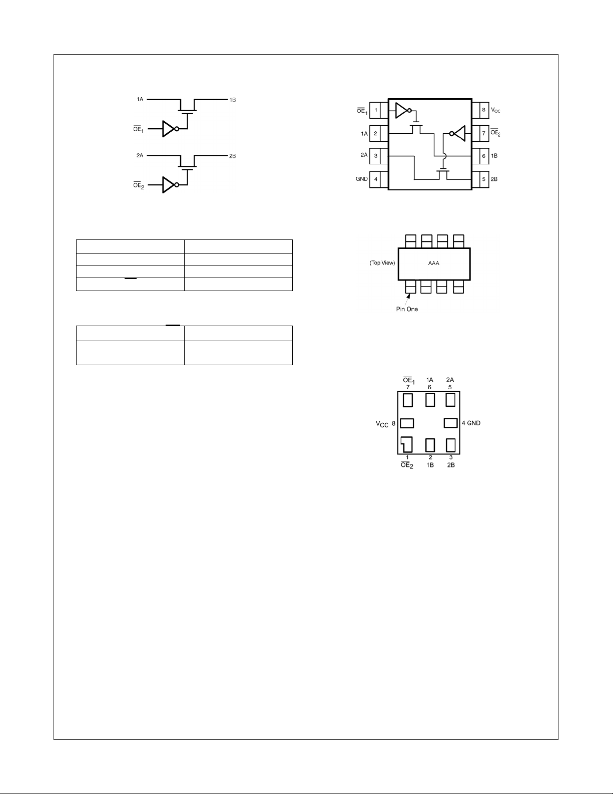
Logic Diagram
NC7WB3125
Pin Descriptions
Pin Name Description
Function Table
Connection Diagrams
ABus A
BBus B
OE
Bus Enable Input
(Top View)
Pin One Orientation Diagra m
Bus Enable Input OE Function
L B Connected to A
H Disconnected
AAA represents Product Code Top Mark - see ordering code
Note: Orientation of Top Mark determines Pin One location. Read the top product
code mark left to right, Pin One is the lower left pin (see diagram).
Pad Assignments for MicroPak
(Top Through View)
www.fairchildsemi.com 2
NC7WB3125
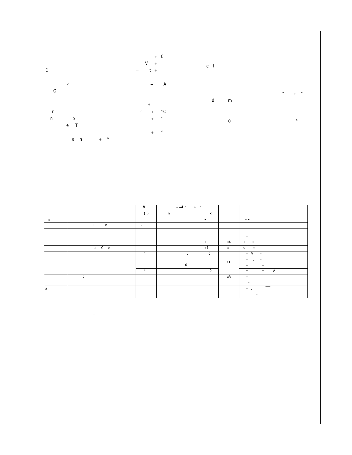
Absolute Maximum Ratings(Note 1)
Supply Voltage (VCC)
DC Switch Voltage (V
DC Output Voltage (V
)
S
) (Note 2)
IN
DC Input Diode Current
) VIN 0V
(I
IK
DC Output (I
or Ground Current
DC V
CC
(I
CC/IGND
Storage Temperature Range (T
) Current 128 mA
OUT
)
STG
Junction Temperature under Bias (T
Junction Lead Temperature (T
)
L
(Soldering, 10 Seconds)
Power Dissipation (P
) @ 85qC 250 mW
D
)
J
0.5V to 7.0V
0.5V to 7.0V
0.5V to 7.0V
65q
C to 150qC
)
50 mA
r
100 mA
150qC
260qC
Recommended Operating
Conditions
Supply Operating (V
Control Input Voltage (V
Switch Input Voltage (V
Output Voltage (V
Operating Temperature (T
Input Rise and Fall Time (t
Switch Control Input 0 ns/V to 5 ns
Switch I/O 0 ns/V to DC
Thermal Resistance (
Note 1: The “Absolute Maximum Ratings” are those values beyond which the safety
of the device cannot be guaranteed. The device should not be operated at these limits. The parametric values defined in the Electrical Characteristics tables are not
guaranteed at the absolute maximum ratings. The “Recommended Operating Conditions” table will define the conditions for actual device operation.
Note 2: The input and output negative voltage ratings may be exceeded if the input
and output diode current ratings are observed.
Note 3: Unused logic inputs must be held HIGH or LOW. They may not float.
(Note 3)
) 4.0V to 5.5V
CC
)0V to 5.5V
IN
)0V to 5.5V
IN
)0V to 5.5V
OUT
)
A
, tf)
r
T
) 250qC/W
JA
DC Electrical Characteristics
V
Symbol Parameter
V
IK
V
IH
V
IL
V
OH
I
IN
I
OFF
R
ON
I
CC
'
I
CC
Note 4: Measured by the voltage drop between A and B pins at the indicated current through the switch. On Resistance is determined by the lower of the
voltages on the two (A or B) pins.
Note 5: Per TTL driven input (VIN 3.4V, control input only). A and B pins do not contribute to ICC.
Clamp Diode Voltage 4.5
HIGH Level Input Voltage 4.0 to 5.5 2.0 V
LOW Level Input Voltage 4.0 to 5.5 0.8 V
HIGH Level Output Voltage 4.0 to 5.5 See Figure 3 V VIN V
Input Leakage Current 5.5
Switch OFF Leakage Current 5.5
Switch On Resistance 4.5 3.0 7.0
(Note 4) 4.5 3.0 7.0 VIN 0V, IIN 30 mA
Quiescent Supply Current 5.5 3.0
Increase in ICC per Input (Note 5) 5.5 1.0 2.5 mA VIN 3.4V, One OE Input only,
CC
(V) Min Typ Max
4.5 6.0 15.0 V
4.0 10.0 20.0 V
TA 40qC to 85qC
Units Conditions
1.2 V IIN 18 mA
r
1.0
r
1.0
P
A0 d VIN d 5.5V
P
A0 d A, B d V
VIN 0V, IIN 64 mA
:
P
2.4V, IIN 15 mA
IN
2.4V, IIN 15 mA
IN
AVIN VCC or GND
I
0
OUT
Other OE V
CC
CC
CC
40q
C to 85qC
3 www.fairchildsemi.com

AC Electrical Characteristics
TA 40qC to 85qC,
Symbol Parameter
NC7WB3125
t
, Propagation Delay Bus-to-Bus 4.0 to 5.5 0.25 ns VI OPEN Figures
PHL
t
PLH
t
PZL
t
PZH
t
PLZ
t
PHZ
Note 6: This parameter is guaranteed by design. The bus switch contributes no propagation delay other than the RC delay of the typical On Resistance of the switch and the 50
pF load capacitance, when driven by an ideal voltage source (zero output impedance). The specified limit is calculated on this basis.
(Note 6)
, Output Enable Time 4.5 to 5.5 0.8 2.5 4.2
, Output Disable Time 4.5 to 5.5 0.8 3.1 4.8
V
CC
(V) Min Typ Max Number
4.0 0.8 3.0 4.6 VI 0V for t
4.0 0.8 2.9 4.4 VI 0V for t
CL 50 pF, RU RD 500
:
Units Conditions Figure
VI 7V for t
ns
VI 7V for t
ns
PZL
PZH
PLZ
PHZ
Capacitance
1, 2
Figures
1, 2
Figures
1Figure 2
Symbol Parameter Typ Max Units Conditions
C
IN
C
I/O
C
I/O
Control Pin Input Capacitance 2.5 pF VCC 0V
(OFF) Port Off Capacitance 6.0 pF VCC 5.0V OE
(ON) Switch ON Capacitance 12.0 pF VCC 5.0V, OE 0V
AC Loading and Waveforms
Input driven by 50: source terminated in 50
includes load and stray capacitance
C
L
Input PRR 1.0 MHz; tW 500 ns
FIGURE 1. AC Test Circuit
:
FIGURE 2. AC Waveforms
www.fairchildsemi.com 4

DC Characteristics
NC7WB3125
FIGURE 3. Typical High Level Output Voltage vs. Supply Voltage
5 www.fairchildsemi.com

Tape and Reel Specification
TAPE FORMAT for US8
Package Tape Number Cavity Cover Tape
NC7WB3125
Designator Section Cavities Status Status
K8X Carrier 250 Filled Sealed
TAPE DIMENSIONS inches (millimeters)
Leader (Start End) 125 (typ) Empty Sealed
Trailer (Hub End) 75 (typ) Empty Sealed
TAPE FORMAT for MicroPak
Package Tape Number Cavity Cover Tape
Designator Section Cavities Status Status
Leader (Start End) 125 (typ) Empty Sealed
L8X Carrier 250 Filled Sealed
Trailer (Hub End) 75 (typ) Empty Sealed
TAPE DIMENSIONS inches (millimeters)
www.fairchildsemi.com 6

REEL DIMENSIONS inches (millimeters)
Tape SizeABCDN W1 W2 W3
8 mm
7.0 0.059 0.512 0.795 2.165 0.331
(177.8) (1.50) (13.00) (20.20) (55.00) (8.40
0.059/0.000 0.567 W1 0.078/0.039
1.50/0.00) (14.40) (W1 2.00/1.00)
NC7WB3125
7 www.fairchildsemi.com

Physical Dimensions inches (millimeters) unless otherwise noted
NC7WB3125
8-Lead US8, JEDEC MO-187, Variation CA 3.1mm Wide
Package Number MAB08A
www.fairchildsemi.com 8

Physical Dimensions inches (millimeters) unless otherwise noted (Continued)
NC7WB3125
Pb-Free 8-Lead MicroPak, 1.6 mm Wide
Package Number MAC08A
9 www.fairchildsemi.com
NC7WB3125 2-Bit Low Power Bus Switch
DISCLAIMER
FAIRCHILD SEMICONDUCTOR RESERVES THE RIGHT TO MAKE CHANGES WITHOUT FURTHER NOTICE TO ANY
PRODUCTS HEREIN TO IMPROVE RELIABILITY, FUNCTION OR DESIGN. FAIRCHILD DOES NOT ASSUME ANY LIABILITY
ARISING OUT OF THE APPLICATION OR USE OF ANY PRODUCT OR CIRCUIT DESCRIBED HEREIN; NEITHER DOES IT
CONVEY ANY LICENSE UNDER ITS PATENT RIGHTS, NOR THE RIGHTS OF OTHERS.
LIFE SUPPORT POLICY
FAIRCHILD’S PRODUCTS ARE NOT AUTHORIZED FOR USE AS CRITICAL COMPONENTS IN LIFE SUPPORT DEVICES
OR SYSTEMS WITHOUT THE EXPRESS WRITTEN APPROVAL OF FAIRCHILD SEMICONDUCTOR CORPORATION
As used herein:
1. Life support devices or systems are devices or systems
which, (a) are intended for surgical implant into the body, or
(b) support or sustain life, or (c) whose failure to perform
when properly used in accordance with instructions for use
provided in the labeling, can be reasonably expected to
result in significant injury to the user.
2. A critical component is any component of a life support
device or system whose failure to perform can be reasonably expected to cause the failure of the life support device
or system, or to affect its safety or effectiveness.
PRODUCT STATUS DEFINITIONS
Definition of terms
Datasheet Identification Product Status Definition
Advance Information Formative or In Design This datasheet contains the design specifications for product develop-
Preliminary First Produc tion This datasheet contains preliminary data, and supplementary data will
No Identification Needed Full Production This datasheet contains final specifications. Fairchild Semiconductor
Obsolete Not In Production This datasheet contains specifications on a product that has been dis-
ment. Specifications may change in any manner without notice.
be published at a later date. Fairchild Semiconductor reserves the right
to make changes at any time without notice in order to improve design.
reserves the right to make changes at any time without notice in order
to improve design.
continued by Fairchild Semiconductor. The datasheet is printed for reference information only.
www.fairchildsemi.com 10
 Loading...