®
NC7SZU04
®
TinyLogic
UHS Unbuffered Inverter
NC7SZU04 — TinyLogic
October 2009
UHS Unbuffrered Inverter
Features
Unbuffered for Crystal Oscillator and Analog
Applications
Balanced Output Drive: ±16mA at 4.5V V
Broad V
Operating Range: 1.65V to 5.5V
CC
CC
Matches Performance of LCX Operated at 3.3V V
Low Quiescent Power: I
T
=25°C
A
<2µA, VCC=5.5V,
CC
Ultra-Small MicroPak™ Packages
Space-Saving SOT23 and SC70 Packages
Description
The NC7SZU04 is a single unbuffered inverter from
Fairchild’s Ultra-High Speed series of TinyLogic®. The
special purpose unbuffered circuit design is primarily
intended for crystal oscillator or analog applications.
The device is fabricated with advanced CMOS
technology to achieve ultra-high speed with high output
CC
drive while maintaining low static power dissipation over
a broad V
operate over the 1.65V to 5.5V V
operating range. The device is specified to
CC
CC
Ordering Information
Part Number Top Mark
NC7SZU04M5X 7ZU4 RoHS 5-Lead SOT23, JEDEC MO-178 1.6mm
NC7SZU04P5X ZU4 RoHS 5-Lead SC70, EIAJ SC-88a, 1.25mm Wide
NC7SZU04L6X C5 RoHS 6-Lead MicroPak™, 1.00mm Wide
NC7SZU04FHX C5 Green 6-Lead, MicroPak2, 1x1mm Body, .35mm Pitch
Eco
Status
Package Packing Method
range.
3000 Units on
Tape & Reel
3000 Units on
Tape & Reel
5000 Units on
Tape & Reel
5000 Units on
Tape & Reel
For Fairchild’s definition of Eco Status, please vis it: http://www.fairchildsemi.com/company/green/rohs_green.html.
© 1996 Fairchild Semiconductor Corporation www.fairchildsemi.com
NC7SZU04 • Rev. 1.0.2

®
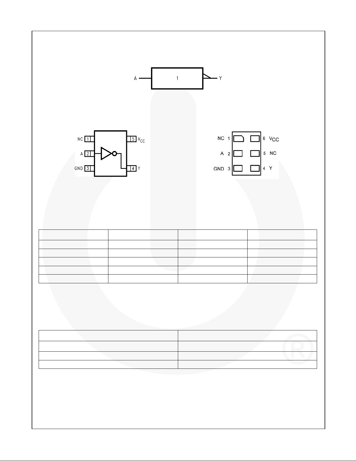
Connection Diagrams
NC7SZU04 — TinyLogic
IEEE/IEC
Figure 1. Logic Symbol
Pin Configurations
Figure 2. SC70 and SOT23 (Top View) Figure 3. MicroPak (Top Through View)
Pin Definitions
Pin # SC70 / SOT23 Pin # MicroPak Name Description
1 1,5 NC No Connect
2 2 A Input
3 3 GND Ground
4 4 Y Output
5 6 VCC Supply Voltage
UHS Unbuffered Inverter
Function Table
Y= /A
Inputs Output
A Y
L H
H L
H = HIGH Logic Level
L = LOW Logic Level
© 1996 Fairchild Semiconductor Corporation www.fairchildsemi.com
NC7SZU04 • Rev. 1.0.2 2

®
NC7SZU04 — TinyLogic
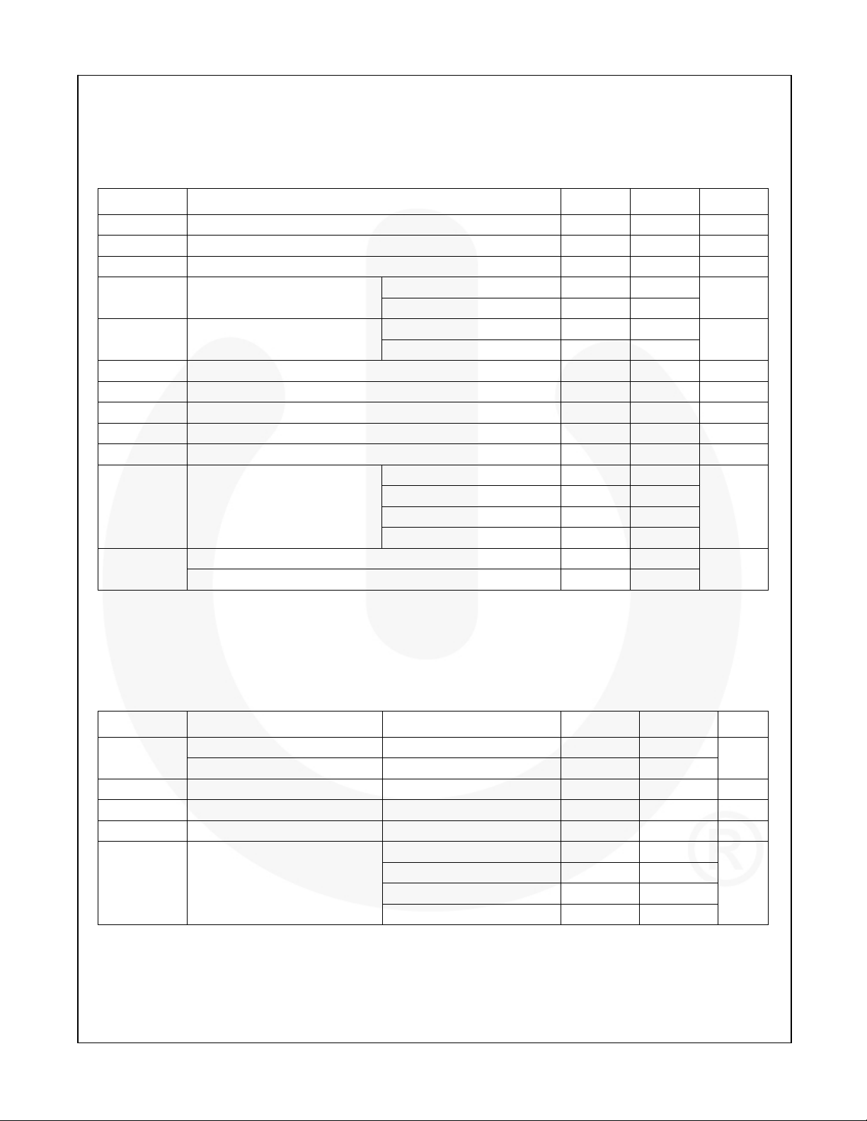
Absolute Maximum Ratings
Stresses exceeding the absolute maximum ratings may damage the device. The device may not function or be
operable above the recommended operating conditions and stressing the parts to these levels is not recommended.
In addition, extended exposure to stresses above the recommended operating conditions may affect device
reliability. The absolute maximum ratings are stress ratings only.
Symbol Parameter Min. Max. Unit
VCC Supply Voltage -0.5 6.0 V
VIN DC Input Voltage -0.5 6.0 V
V
DC Output Voltage -0.5 6.0 V
OUT
< -0.5V -50
V
IIK DC Input Diode Current
IOK DC Output Diode Current
I
DC Output Current ±50 mA
OUT
ICC or I
DC VCC or Ground Current ±100 mA
GND
T
Storage Temperature Range -65 +150 °C
STG
IN
VIN > VCC+5.0V +20
< -0.5V -50
V
OUT
V
> 0.5V, VCC=GND +50
OUT
TJ Junction Temperature Under Bias +150 °C
TL Junction Lead Temperature (Soldering, 10 Seconds) +260 °C
SOT-23 200
PD Power Dissipation at +85°C
SC70-5 150
MicroPak-6 130
MicroPak2-6 120
ESD
Human Body Model, JEDEC:JESD22-A114 4000
Charge Device Model, JEDEC:JESD22-C101 2000
mA
mA
mW
V
UHS Unbuffered Inverter
Recommended Operating Conditions
The Recommended Operating Conditions table defines the conditions for actual device operation. Recommended
operating conditions are specified to ensure optimal performance to the datasheet specifications. Fairchild does not
recommend exceeding them or designing to Absolute Maximum Ratings.
Symbol Parameter Conditions Min. Max. Unit
VCC
VIN Input Voltage 0 5.5 V
V
OUT
TA Operating Temperature -40 +85 °C
θ
JA
Note:
1. Unused inputs must be held HIGH or LOW. They may not float.
© 1996 Fairchild Semiconductor Corporation www.fairchildsemi.com
NC7SZU04 • Rev. 1.0.2 3
Supply Voltage Operating 1.65 5.50
Supply Voltage Data Retention 1.50 5.50
V
Output Voltage 0 VCC V
SOT-23 300
Thermal Resistance
SC70-5 425
MicroPak-6 500
°C/W
MicroPak2-6 560
 Loading...