Fairchild NC7SZ86 service manual

NC7SZ86
TinyLogic£ UHS 2-Input Exclusive-OR Gate
NC7SZ86 TinyLogic£ UHS 2-Input Exclusive-OR Gate
October 1996
Revised February 2005
General Description
The NC7SZ86 is a single 2-I nput Exclusive- OR Gate from
Fairchild's Ultra High Speed Series of TinyLogic
device is fabricated w ith advanced CMOS technology to
achieve ultra high spe ed w ith high output drive whi le ma i ntaining low static power dissipation over a very broad V
operating range. Th e device is specified to operate ov er
the 1.65V to 5.5V V
high impedance when V
up to 6V independent of V
range. The inputs and output are
CC
is 0V. Inputs tolerate voltages
CC
operating voltage.
CC
£
. The
Features
■ Space saving SOT23 or SC70 5-lead package
■ Ultra small MicroPak
■ Ultra High Speed; t
■ High Output Drive;
CC
■ Broad V
■ Matches the performance of LCX when operated at 3.3V
■ Power down high impedance inputs/output
■ Overvoltage tolerant inputs facilitate 5V to 3V translation
■ Patented noise/EMI reduction circuitry implemented
Operating Range; 1.65V to 5.5V
CC
¥
Pb-Free leadless package
2.9 ns typ into 50 pF at 5V V
PD
r
24 mA at 3V V
CC
CC
Ordering Code:
Order Package Product Code
Number Number Top Mark
NC7SZ86M5X MA05B 7Z86 5-Lead SOT23, JEDEC MO-178, 1.6mm 3k Units on Tape and Reel
NC7SZ86M5X_NL MA05B 7Z86 Pb-Free 5-Lead SOT23, JEDEC MO-178,
NC7SZ86P5X MAA05A Z86 5-Lead SC70, EIAJ SC-88a, 1.25mm Wide 3k Units on Tape and Reel
NC7SZ86P5_NL
(Note 1)
NC7SZ86P5X_NL
(Note 2)
NC7SZ86L6X MAC06A B3 Pb-Free 6-Lead MicroPak, 1.0mm Wide 5k Units on Tape and Reel
Pb-Free package per JEDEC J-STD-020B.
Note 1: “_NL” indicates lead-free product (per JEDEC J-STD-020B).
Note 2: “_NL” indicates lead-free product (per JEDE C J -ST D -020B). Device is av ailable in Tape and Reel only.
MAA05A Z86 Pb-Free 5-Lead SC70, EIAJ SC-88a,
MAA05A Z86 Pb-Free 5-Lead SC70, EIAJ SC-88a,
1.6mm
1.25mm Wide
1.25mm Wide
Package Description Supplied As
3k Units on Tape and Reel
3k Units on Tape and Reel
3k Units on Tape and Reel
£
is a registered trademark of Fairchild Semiconductor Corpo ration.
TinyLogic
¥
is a trademark of Fair ch ild Semiconductor Co rporation.
MicroPak
© 2005 Fairchild Semiconductor Corporation DS012164 www.fairchildsemi.com

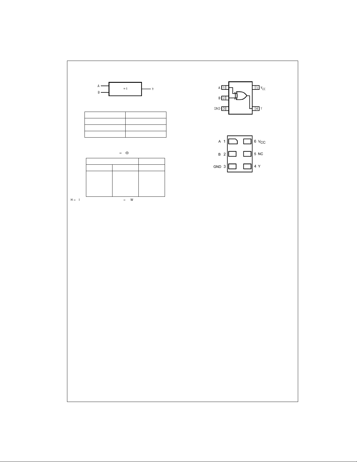
Logic Symbol
Connection Diagrams
IEEE/IEC
NC7SZ86
Pin Descriptions
Pin Names Description
A, B Input
YOutput
NC No Connect
Function Table
Y AB
Inputs Output
ABY
LLL
LHH
HLH
HHL
H HIGH Logic Level L LOW Logic Level
Pin Assignments for SC70 and SOT23
(Top View)
Pad Assignments for MicroPak
(Top Thru View)
www.fairchildsemi.com 2

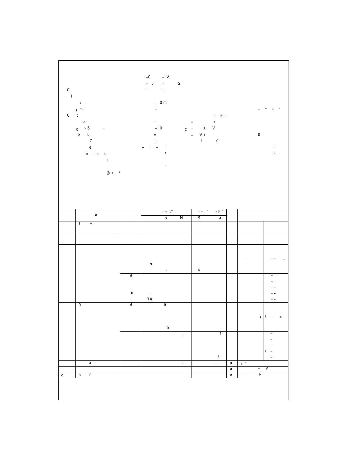
Absolute Maximum Ratings(Note 3) Recommended Operating
Supply Voltage (VCC)
DC Input Voltage (V
DC Output Voltage (V
DC Input Diode Current (I
0.5V
@V
IN
@ V
! 6V
IN
DC Output Diode Current (I
0.5V
@V
OUT
@ V
! 6V, VCC GND
OUT
DC Output Current (I
/GND Current (ICC/I
DC V
CC
Storage Temperature (T
IN
)
OUT
OUT
)
STG
)
)
IK
)
OK
)
GND
)
Junction Temperature under Bias (T
Junction Lead Temperature (T
);
L
0.5V to 6V
0.5V to 6V
0.5V to 6V
r
50 mA
r
50 mA
65qC–
) 150qC
J
(Soldering, 10 seconds) 260
Power Dissipation (P
) @ 85qC
D
SOT23-5 200 mW
SC70-5 150 mW
50 mA
20 mA
50 mA
20 mA
150qC
Conditions
Supply Voltage Operating (V
Supply Voltage Data Retention (V
Input Voltage (V
Output Voltage (V
Operating Temperature (TA)
Input Rise and Fall Time (t
1.8V, 2.5V r0.2V 0 ns/V–20 ns/V
V
CC
V
3.3V r 0.3V 0 ns/V–10 ns/V
CC
5.0V r 0.5V 0 ns/V–5 ns/V
V
CC
Thermal Resistance (
SOT23-5 300
SC70-5 425
Note 3: Absolute maximum ratings are DC values beyond which t he devi ce
q
C
may be damaged or have its useful life impaired. The datasheet specifications should be met, without exception, to ensure that the system design is
reliable over its power supply, temperature, and output/input loading variables. Fairchild doe s not recomme nd operation ou tside datasheet spe cifications.
Note 4: Unused inputs must be held HIGH or LOW. They may not float.
(Note 4)
) 1.65V to 5.5V
CC
) 1.5V to 5.5V
) 0V to 5.5V
IN
)0V to V
OUT
T
JA
CC
, tf)
r
)
DC Electrical Characteristics
V
Symbol Parameter
V
HIGH Level Input Voltage 1.65 to 1.95 0.75 V
IH
V
LOW Level Input Voltage 1.65 to 1.95 0.25 V
IL
V
HIGH Level Output Voltage 1.65 1.55 1.65 1.55
OH
V
LOW Level Output Voltage 1 .65 0.0 0.1 0.1
OL
I
Input Leakage Current 0 to 5.5
IN
I
Power Off Leakage Current 0.0 1 10
OFF
I
Quiescent Supply Current 1.65 to 5.5 2.0 20
CC
CC
(V) Min Typ Max Min Max
2.3 to 5.5 0.7 V
2.3 to 5.5 0.3 V
1.8 1.7 1.8 1.7
2.3 2.2 2.3 2.2
3.0 2.9 3.0 2.9
4.5 4.4 4.5 4.4
1.65 1.29 1.52 1.29
2.3 1.9 2.15 1.9 I
3.0 2.4 2.80 2.4 IOH 16 mA
3.0 2.3 2.68 2.3 IOH 24 mA
4.5 3.8 4.20 3.8 IOH 32 mA
1.8 0.0 0.1 0.1
2.3 0.0 0.1 0.1
3.0 0.0 0.1 0.1
4.5 0.0 0.1 0.1
1.65 0.08 0.24 0.24
2.3 0.10 0.3 0.3 IOL 8 mA
3.0 0.15 0.4 0.4 IOL 16 mA
3.0 0.22 0.55 0.55 IOL 24 mA
4.5 0.22 0.55 0.55 IOL 32 mA
TA 25qCT
CC
CC
A
0.75 V
0.7 V
CC
CC
r
1
40qC to 85qC
CC
CC
0.25 V
0.3 V
CC
r
10PAVIN 5.5V, GND
Units Conditions
V
CC
V
VV
VIH, VILIOH 100 PA
IN
V
VVIN VIH or VILIOL 100 PA
V
P
AVIN or V
P
AVIN 5.5V, GND
40qC–85q
5.5V
OUT
CC
C
q
C/W
q
C/W
IOH 4 mA
8 mA
OH
IOL 4 mA
NC7SZ86
3 www.fairchildsemi.com
 Loading...