Fairchild NC7SZ34 service manual

®
NC7SZ34
TinyLogic
®
UHS Buffer
NC7SZ34 — TinyLogic
February 2011
UHS Buffer
Features
Ultra-High Speed: t
at 5V V
CC
High Output Drive: ±24mA at 3V V
Broad V
Operating Range: 1.65V to 5.5V
CC
2.4ns (Typical) into 50pF
PD
CC
Matches Performance of LCX Operated at 3.3V V
Power-Down High-Impedance Inputs / Outputs
Description
The NC7SZ34 is a single buffer from Fairchild’s UltraHigh Speed (UHS) series of TinyLogic
fabricated with advanced CMOS technology to achieve
ultra-high speed with high output drive, while
maintaining low static power dissipation over a broad
V
operating range of 1.65V to 5.5V VCC. The inputs
CC
CC
and output are high-impedance when V
tolerate voltages up to 7V, independent of V
voltage.
®
. The device is
is 0V. Inputs
CC
operating
CC
Proprietary Noise / EMI Reduction Circuitry
WLCSP Package
Related Resources
AN-5055 — Portability and Ultra Low Power
TinyLogic®
MS-503 — Family Characteristics TinyLogic
HS/HST and UHS Series
Ordering Information
Part Number Top Mark Package Packing Method
NC7SZ34UCX KJ
4-Lead, Wafer-Level Chip Scale 0.76x0.76x0.5mm
Wafer-Level Chip-Scale Package (WLCSP)
3000 Units on
Tape & Reel
®
© 2010 Fairchild Semiconductor Corporation www.fairchildsemi.com
NC7SZ34 • Rev. 1.0.1

®
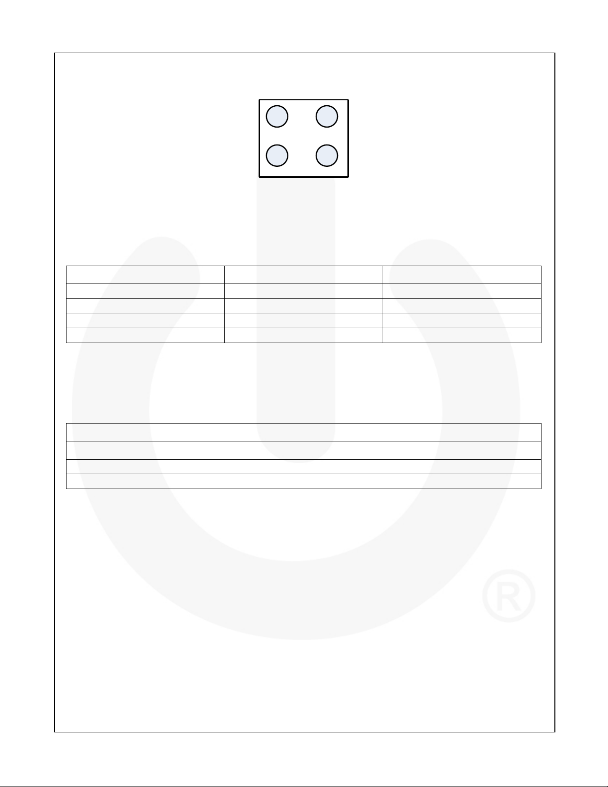
Pin Configurations
NC7SZ34 — TinyLogic
A1 A2
B2B1
Pin Definitions
WLCSP Name Description
A1 A Input
A2 VCC Power Supply
B1 GND Ground
B2 Y Output
Function Table
Y= A
LOW Logic Level LOW Logic Level
HIGH Logic Level HIGH Logic Level
Figure 1. WLCSP (Top View)
Inputs Output
A Y
UHS Buffer
© 2010 Fairchild Semiconductor Corporation www.fairchildsemi.com
NC7SZ34 • Rev. 1.0.1 2

®
NC7SZ34 — TinyLogic
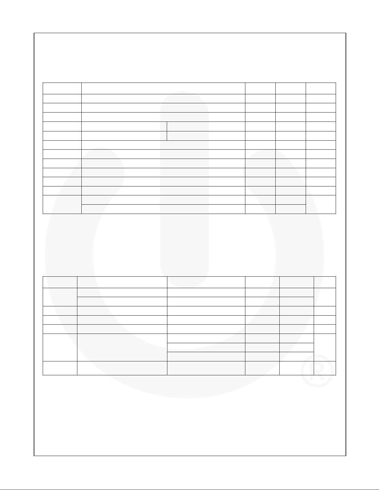
Absolute Maximum Ratings
Stresses exceeding the absolute maximum ratings may damage the device. The device may not function or be
operable above the recommended operating conditions and stressing the parts to these levels is not recommended.
In addition, extended exposure to stresses above the recommended operating conditions may affect device reliability.
The absolute maximum ratings are stress ratings only.
Symbol Parameter Min. Max. Unit
VCC Supply Voltage -0.5 7.0 V
VIN DC Input Voltage -0.5 7.0 V
V
DC Output Voltage -0.5 7.0 V
OUT
IIK DC Input Diode Current VIN < -0.5V -50 mA
IOK DC Output Diode Current V
I
DC Output Current ±50 mA
OUT
ICC or I
DC VCC or Ground Current ±50 mA
GND
T
Storage Temperature Range -65 +150 °C
STG
< -0.5V -50 mA
OUT
TJ Junction Temperature Under Bias +150 °C
TL Junction Lead Temperature (Soldering, 10 Seconds) +260 °C
PD Power Dissipation at +85°C 200 mW
ESD
Human Body Model, JEDEC:JESD22-A114 4000
Charge Device Model, JEDEC:JESD22-C101 2000
V
UHS Buffer
Recommended Operating Conditions
The Recommended Operating Conditions table defines the conditions for actual device operation. Recommended
operating conditions are specified to ensure optimal performance to the datasheet specifications. Fairchild does not
recommend exceeding them or designing to Absolute Maximum Ratings.
Symbol Parameter Conditions Min. Max. Unit
VCC
VIN Input Voltage 0 5.5 V
V
OUT
TA Operating Temperature -40 +85 °C
tr, tf Input Rise and Fall Times
JA
Note:
1. Unused inputs must be held HIGH or LOW. They may not float.
Supply Voltage Operating 1.65 5.50
Supply Voltage Data Retention 1.5 5.5
V
Output Voltage 0 VCC V
V
at 1.8V, 2.5V ±0.2V 0 20
CC
VCC at 3.3V ±0.3V 0 10
ns/V
VCC at 5.0V ±0.5V 0 5
Thermal Resistance 80 °C/W
© 2010 Fairchild Semiconductor Corporation www.fairchildsemi.com
NC7SZ34 • Rev. 1.0.1 3
 Loading...