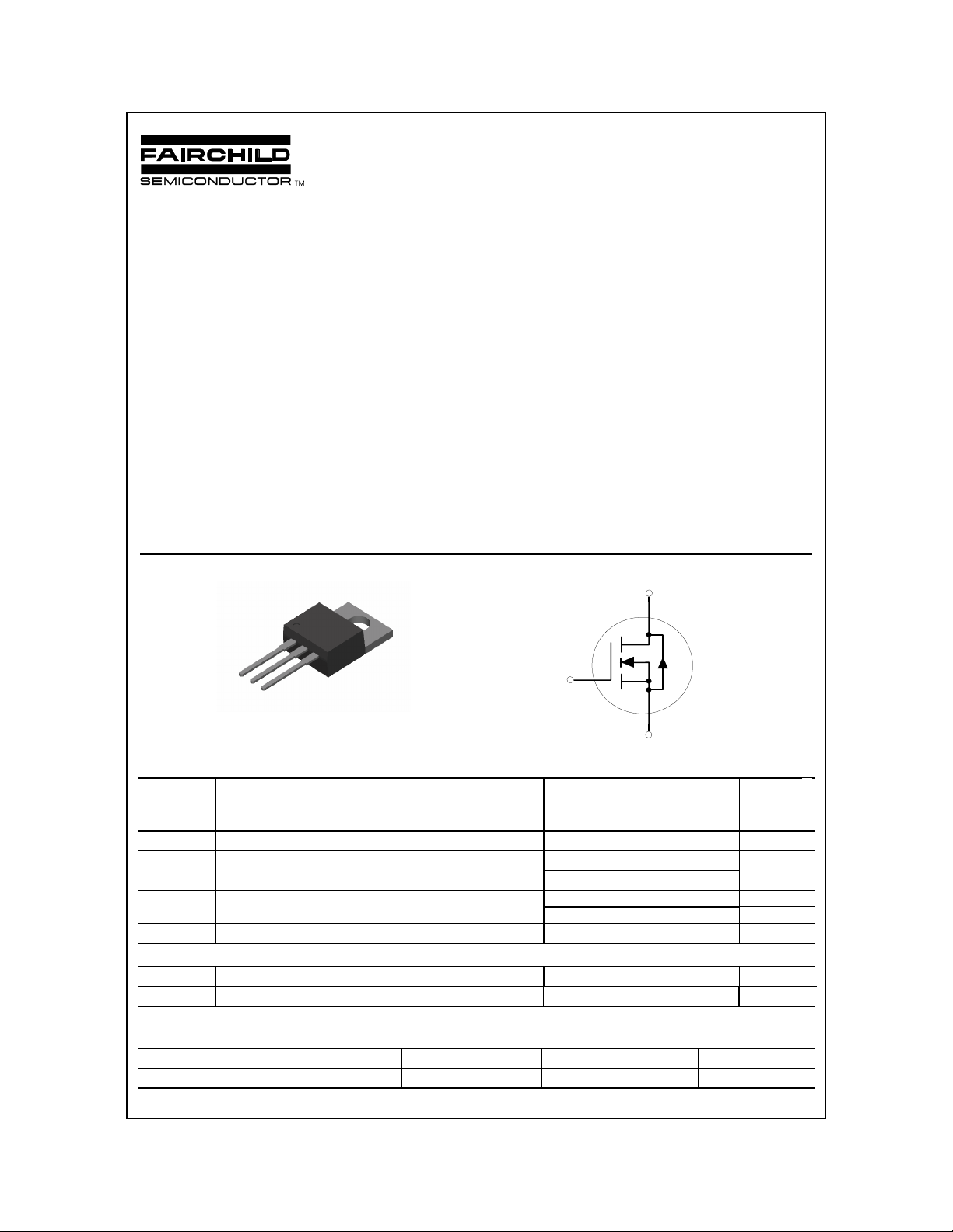
Fairchild MTP3055VL service manual

DISTRIBUTION GROUP*
MTP3055VL
N-Channel Logic Level Enhancement Mode Field Effect T ransistor
MTP3055VL
June 2000
General Description
This N-Channel Logic Level MOSFET has been designed
specifically for low voltage, high speed switching
applications i.e. power supplies and power motor
controls.
This MOSFET features faster switching and lower gate
charge than other MOSFETs with comparable R
specifications.
The result is a MOSFET that is easy and safer to drive
(even at very high frequencies).
G
D
TO-220
DS(ON)
S
Features
• 12 A, 60 V. R
• Critical DC electrical parameters specified at elevated
temperature.
• Low drive requirements allowing operation directly from
logic drivers. Vgs(th) < 2 V.
• Rugged internal source-drain diode can eliminate the
need for an external Zener diode transient suppressor.
• 175°C maximum junction temperature rating.
= 0.18 Ω @ VGS = 5 V
DS(ON)
D
G
Absolute Maximum Ratings
TC = 25°C unless otherwise noted
Symbol Parameter
V
DSS
V
GSS
I
D
D
TJ, T
STG
Drain-Source Voltage 60 V
Gate-Source Voltage
Drain Current - Continuous 12 A
- Pulsed 42
Power Dissipation @ TC = 25°C48WP
Derate above 25°C0.32W/
Operating and Storage Junction Temperature Range -65 to +175
Thermal Characteristics
R
JC
θ
R
JA
θ
Thermal Resistance, Junction-to- Case 3.13
Thermal Resistance, Junction-to- Ambient
Package Outlines and Ordering Information
Device Marking Device Package Information Quantity
MTP3055VL MTP3055VL Rails/Tubes 45 units
Die and manufacturing source subject to change without prior notific ation
*
1999 Fairchild Semiconductor Corporation
(Note 1)
S
Ratings
15 V
±
62.5
.
Units
C
°
C
°
C/W
°
C/W
°
MTP3055VL Rev. A1

MTP3055VL
Electrical Characteristics
TC = 25°C unless otherwise noted
Symbol Parameter Test Conditions Min Typ Max Units
DRAIN-SOURCE AVALANCHE RATINGS
w
DSS
I
AR
Single Pulse Drain-Source
Avalanche Energy
Maximum Drain-Source Avalanche Current 12 A
(Note 2)
VDD = 25 V, ID = 12 A 72 mJ
Off Characteristics
BV
DSS
∆
BV
∆
T
I
DSS
I
GSSF
I
GSSR
On Characteristics
V
GS(th)
∆
GS(th)
V
∆
T
R
DS(on)
V
DS(on)
g
FS
Drain-Source Breakdown
Voltage
Breakdown Voltage Temperature
DSS
Coefficient
J
= 0 V, ID = 250 µA
V
GS
= 250 µA, Referenced to 25°C
I
D
60 V
55
Zero Gate Voltage Drain Current VDS = 60 V, VGS = 0 V 10
VDS = 60 V, VGS = 0 V, TJ =
150°C
Gate-Body Leakage Current,
VGS = 15 V, VDS = 0 V 100 nA
Forward
Gate-Body Leakage Current,
VGS = -15 V, VDS = 0 V -100 nA
Reverse
(Note 2)
Gate Threshold Voltage
Gate Threshold Voltage
Temperature Coefficient
J
Static Drain-Source
V
= VGS, ID = 250 µA
DS
= 250 µA, Referenced to 25°C
I
D
11.62 V
-4
VGS = 5 V,ID = 6 A, 0.100 0.180
On-Resistance
Drain-Source On-Voltage
VGS = 5 V,ID = 12 A 2.6 V
On-Resistance
Forward Transconductance VDS = 8 V, ID = 6 A 5 8.7 S
mV/°C
µ
100
mV/°C
A
Ω
Dynamic Characteristics
C
iss
C
oss
C
rss
Switching Characteristics
t
d(on)
t
r
t
d(off)
t
f
Q
g
Q
gs
Q
gd
Input Capacitance 345 570 pF
Output Capacitance 110 160 pF
= 25 V, VGS = 0 V,
V
DS
f = 1.0 MHz
Reverse Transfer Capacitance
(Note 2)
Turn-O n D ela y T ime 20 ns
Turn-O n R ise T ime 190 ns
= 30 V, ID = 12 A,
V
DD
V
GS
= 5 V, R
GEN
= 9.1
Ω
Turn-O ff D ela y T ime 30 ns
Turn-O ff F all Time
Total Gate Charge 7.8 10 nC
Gate-Source Charge 1.7 nC
= 48 V,
V
DS
= 12 A, VGS = 5 V
I
D
Gate-D ra in C h a rge
Drain-Source Diode Characteristics and Maximum R atings
I
S
I
SM
V
SD
Maximum Continuous Drain-Source Diode Forward Current
Maximum Pulsed Drain-Source Diode Forward Current
Drain-Source Diode Forward
Voltage
t
rr
Drain-Source Reverse Recovery
Time
Notes:
1. R
is the sum of the juntion-to-case and case-to-ambient thermal resistance.
θJA
2. Pulse Test: Pulse Width ≤ 300 µs, Duty Cycle ≤ 2.0%
VGS = 0 V, IS = 12 A
=12 A, di/dt = 100A/µs
I
F
(Note 2)
(Note 2)
(Note 2)
30 40 pF
90 ns
3.2 nC
12 A
42 A
1.3 V
55 nS
MTP3055VL Rev. A1
 Loading...