Application Note AN-9056
Using Fairchild Semiconductor Dual CoolTM
MOSFETs
Dennis Lang
INTRODUCTION
Pursuing a strategy of power density leadership,
Fairchild Semiconductor has released a new
power specific packaging technology, Dual
CoolTM, to meet the rigors of escalating demand
for more improved thermal management in
electronics designs. This technology creates a
direct heat path from both the drain and source
sides of the vertical MOSFET die structure
through the addition of a heat slug to the top of
the package. This structure allows for
supplemental cooling on the top of the package
with a heat sink system in addition to the direct
conduction path in to the printed circuit board.
This application note will describe the package
construction, address thermal characterization
challenges and offer some systemic examples
utilizing heat sinks.
PACKAGE CONSTRUCTION
Dual Cool package construction is an
evolutionary concept based on contemporary
customer packaging form factor preferences,
and incorporating new features to meet future
performance expectations. The package design
team chose to keep the very popular Power33
and Power56 lead geometries and pin outs
allowing customers to add heat sinkable
performance to existing PCB pad designs.
Customers currently using a heat sink on the
surface of a PowerQFN package will find this a
very useful feature. Dual Cool uses 4 mils thin
silicon as the core package design constraint.
This represents half the thickness of the typical
MOSFET which traditionally used 8 mils thick
silicon dice. By reducing the die thickness to 4
mils, thermal and electrical performance are
improved by reducing the parasitic resistance
created by the bulk resistance from the doped
silicon area electrons flow through to get from
the trench structure at the top of the wafer to the
drain lead frame connection at the bottom. The
top and bottom surfaces of the die are plated
with solderable metal to permit solder
attachment of the drain lead frame on the
bottom, and the source and gate clips on the top.
To improve the heat transfer path from the die to
the top of the package for use with a heat sink, a
heat slug is soldered to the source clip and
exposed on the top of the package to interface
with a heat sink.
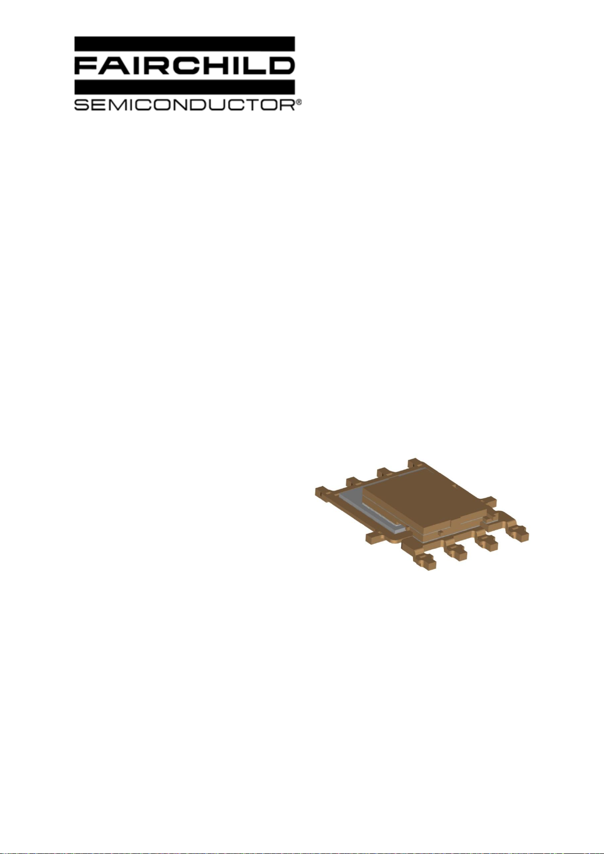
Figure 1: Solid model illustrating Dual Cool
package construction.
Solder attachment of the silicon to the lead
frames, with optimized copper clips additionally
reduces electrical and thermal parasitics. The
, that is, the thermal resistance from the
JC
junction to the case has two important values
with this package type, the junction to case
thermal resistance to the drain tab as well as the
top heat slug. The datasheet offers these values
for each specific product type. These numbers
are a measure of the two efficient heat paths out
of the component, giving the designer options for

managing the heat loads created by high power
density for designs.
CHALLENGE FOR BOARD DESIGNERS
The majority of consumer electronics designers
use FR-4 board material for their designs. FR-4
employs a resin system that has a glass
transition temperature (Tg) typically in the range
of 115-125ºC. This is the lowest Tg material in
most consumer electronics products, thus setting
the limit for temperatures in operation. Reaching
the glass transition temperature can see a
radical transition of FR-4 material properties,
including a four-fold increase in the out of plane
(or Z-axis) coefficient of thermal expansion
(CTE). The exponential increase in CTE results
in multiplied stresses on board to component
solder joints, and plated through holes in the
PCB. High aspect ratio plated through holes,
relatively small holes to large board thicknesses,
lead to boards that are particularly sensitive to
temperature excursions above Tg. To avoid this
scenario many designers strive to limit their
board temperatures at 100ºC, creating safety
factor in the design. With the long term reliability
of their products directly related to thermal
management, designers need effective tools to
characterize their designs.
TEST METHODOLOGY
This device presents a challenge for thermal
characterization on an end user‟s board. An
increasingly popular way for power designers to
characterize their designs is using infrared
thermographs. This technique works well with
normal PowerQFN devices as the plastic mold
compound is semi-transparent to infrared,
presents a relatively consistent case emissivity
of approximately 0.92, and with thin ( 1.0mm)
plastic molded components, the camera often
yields temperatures within 5-10% of junction
temperature. By allowing for the particulars of
using an infrared camera, the designer can
quickly and precisely determine the important
temperatures in a system without a heat sink
during design optimization and verification.
When power packages of any kind are used with
a heat sink, a challenge is presented to the
engineer or technician who would opt to use this
method. The heat sink is not transparent to
infrared, preventing the camera from capturing
accurate temperatures of the device junction.
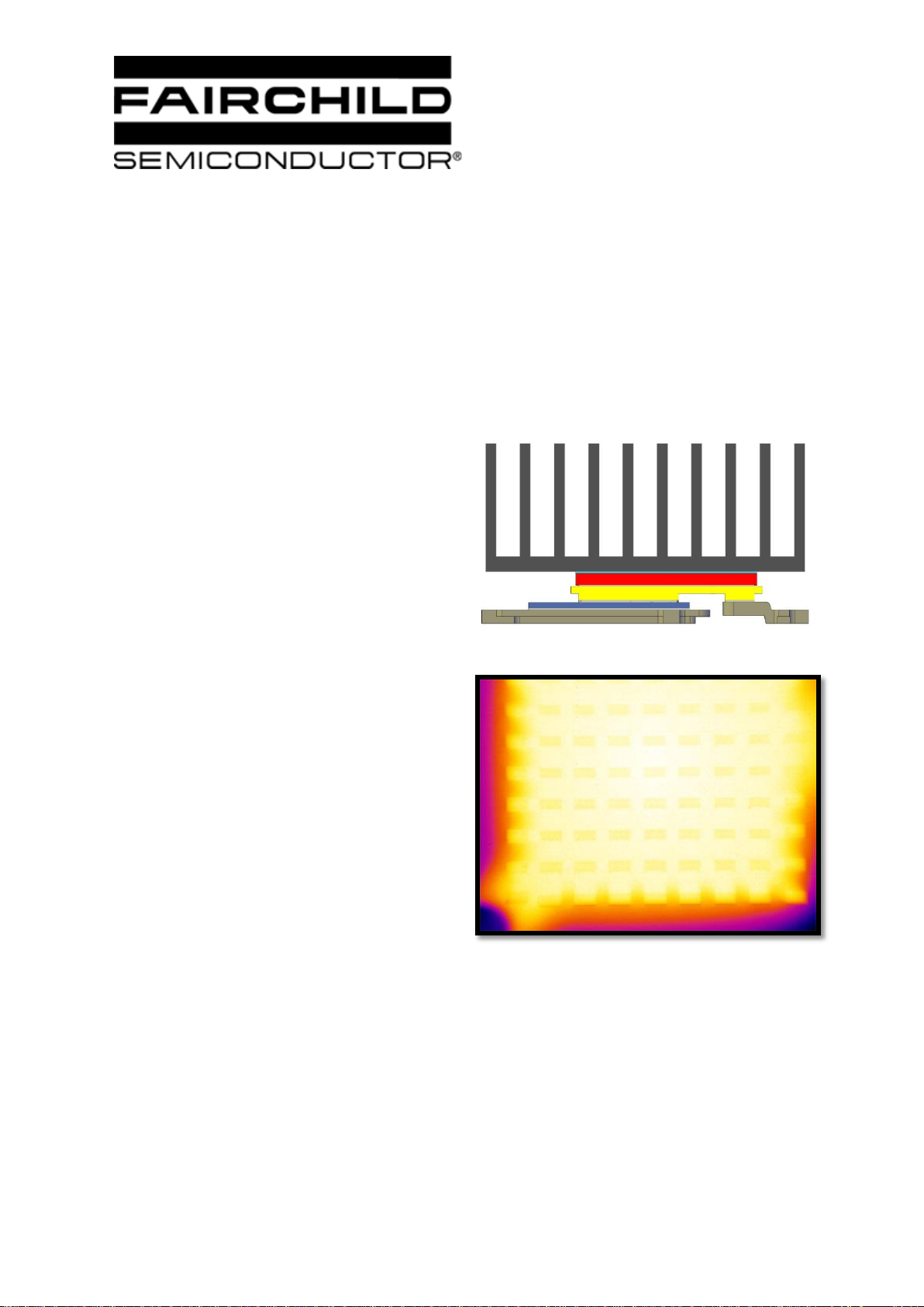
Figure 2: Cross section of Dual Cool and heat
sink assembly.
Figure 3: Thermograph of Dual Cool with
heat sink in operation.
To measure the temperature of various devices
under test, a method for attaching a
thermocouple to the drain pad was devised. This
method should be as close to the die as possible
to assure that surrounding components, airflow,
and other factors do not affect thermocouple
readings. Attempts to correlate temperature to a

location on the surface copper layer near the
component proved untenable. Heat transfer is a
non-linear function over distance and varying
load and environmental conditions may render a
correlation incorrect over the range of use
conditions the board is characterized across. To
address these concerns, it is desirable to locate
the thermocouple as near the silicon die as
possible.
An unplated via can be drilled in the drain pad of
verification boards for insertion of a
thermocouple to touch the drain lead of the
device. This via should not be plated, otherwise,
during SMT processing, solder will wick down
the copper and foul the opening for the
thermocouple. The via should be kept as small
as possible, but be large enough to use the
thermocouple size desired. The boards used in
this experiment had a 28 mils diameter hole
drilled. The boards designed for this study were
all single layer. If the board to be tested is
multilayer, it is a good idea to create a keep out
in the copper planes of all layers for the drilled
hole to assure there is no shorting of layers
through the thermocouple wire.
As the Dual Cool package was designed to
duplicate the industry standard PCB pad for
3.3x3.3mm and 5x6mm PowerQFNs, the same
footprint and PCB design was used to directly
compare wire bonded, clip bonded and Dual
Cool products at thermal steady state. The
board was constructed of lead free rated, 62 mils
thick FR-4 material.
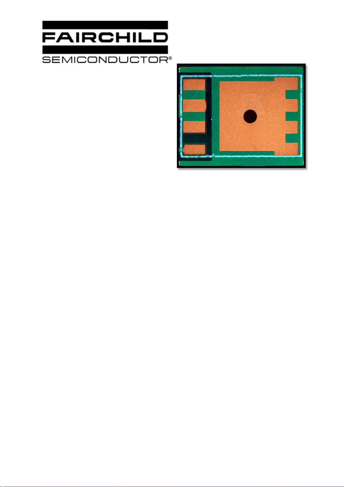
Figure 4: Power56 PCB pad with unplated
hole for thermocouple.
It may occur to the designer that this hole could
reduce thermal or electrical performance. As up
to 25% voiding is acceptable in the device this
was not considered a problematic concern for a
verification board. Of more concern is the ability
of the thermocouple wires to act as a heat sink
and remove enough heat from the board to
under-predict temperatures during operation in
the end application. This leads to the first
reported experiment, attempting to address the
question, can larger thermocouples change the
results of the experiment?
DEVICES CHOSEN FOR ALL
EXPERIMENTS
The devices used in this experiment were meant
to be as similar as possible, to make the
differences in thermal performance attributable
to the package technologies exclusively.
Compared in this paper will be components with
traditional bond wires used to make the gate and
source connections, a clip-bonded product,
using soldered copper clips to make the gate
and source connections, and the Dual Cool
package described in detail previously. All three
components used employ 4 mil thick die. The
die used in the chosen Dual Cool and clip
 Loading...