Fairchild MOCD207M service manual

MOCD207M, MOCD208M — Dual Channel Phototransistor Small Outline Surface Mount Optocouplers
April 2009
MOCD207M, MOCD208M
Dual Channel Phototransistor Small Outline Surface
Mount Optocouplers
Features
■
Dual channel optocoupler
Convenient plastic SOIC-8 surface mountable
■
package style
■
Tw o channels in one compact surface mount package
Closely matched current transfer ratios to minimize
■
unit-to-unit variation
■
Minimum V
Standard SOIC-8 footprint, with 0.050” lead spacing
■
■
Compatible with dual wave, vapor phase and IR reflow
soldering
High input-output isolation of 2500 Vac (rms)
■
guaranteed
Meets U.L. regulatory requirements, file #E90700,
■
volume 2
(BR)CEO
of 70 volts guaranteed
Applications
■
Feedback control circuits
■
Interfacing and coupling systems of different
potentials and impedances
■
General purpose switching circuits
Monitor and detection circuits
■
Description
The MOCD207M/MOCD208M consist of two silicon
phototransistors optically coupled to two GaAs infrared
LEDs. These devices are constructed in a small outline
surface mount package which conforms to the standard
SOIC-8 footprint.
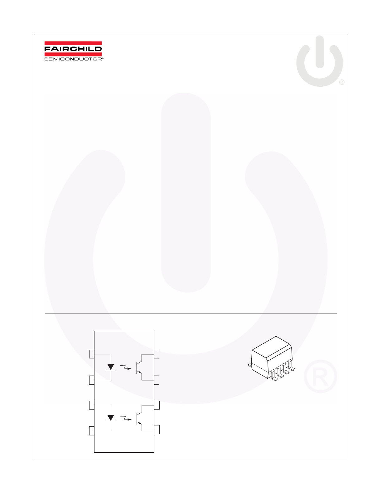
Schematic Package
ANODE 1
CATHODE 1
ANODE 2
CATHODE 2
©2003 Fairchild Semiconductor Corporation www.fairchildsemi.com
MOCD207M, MOCD208M Rev. 1.0.6
1
2
3
4
8
COLLECTOR 1
EMITTER 1
7
6
COLLECTOR 2
5
EMITTER 2

MOCD207M, MOCD208M — Dual Channel Phototransistor Small Outline Surface Mount Optocouplers
Absolute Maximum Ratings
(T
= 25°C unless otherwise specified)
A
Stresses exceeding the absolute maximum ratings may damage the device. The device may not function or be
operable above the recommended operating conditions and stressing the parts to these levels is not recommended.
In addition, extended exposure to stresses above the recommended operating conditions may affect device reliability.
The absolute maximum ratings are stress ratings only.
Symbol Rating Value Unit
EMITTER
I
F
I
(pk) Forward Current – Peak (PW = 100µs, 120pps) 1.0 A
F
V
R
P
D
DETECTOR
V
CEO
V
CBO
V
ECO
I
C
P
D
TOTAL DEVICE
V
ISO
P
D
T
A
T
stg
T
L
Forward Current – Continuous 60 mA
Reverse Voltage 6.0 V
LED Power Dissipation @ T
Derate above 25°C
= 25°C
A
90
0.8
mW
mW/°C
Collector-Emitter Voltage 70 V
Collector-Base Voltage 70 V
Emitter-Collector Voltage 7.0 V
Collector Current-Continuous 150 mA
Detector Power Dissipation @ T
Derate above 25°C
Input-Output Isolation Voltage
A
(1, 2)
= 25°C
150
1.76
mW
mW/°C
2500 Vac(rms)
(f = 60Hz, 1 min. Duration)
Total Device Power Dissipation @ T
Derate above 25°C
= 25°C
A
250
2.94
mW
mW/°C
Ambient Operating Temperature Range -40 to +100 °C
Storage Temperature Range -40 to +125 °C
Lead Soldering Temperature (1/16” from case,
260 °C
10 sec. duration)
©2003 Fairchild Semiconductor Corporation www.fairchildsemi.com
MOCD207M, MOCD208M Rev. 1.0.6 2

≤
Ω
MOCD207M, MOCD208M — Dual Channel Phototransistor Small Outline Surface Mount Optocouplers
Electrical Characteristics
(T
= 25°C unless otherwise specified)
A
(3)
Symbol Parameter Test Conditions Device Min. Typ.* Max. Unit
EMITTER
V
Input Forward Voltage I
F
I
Reverse Leakage Current V
R
C Capacitance All 18 pF
DETECTOR
I
CEO
I
CEO
V
(BR)CEO
Collector-Emitter Dark Current V
Collector-Emitter Breakdown
Voltage
V
(BR)CEO
Emitter-Collector Breakdown
Voltage
C
Collector-Emitter Capacitance f = 1.0 MHz, V
CE
COUPLED
CTR Current Transfer Ratio,
Collector to Emitter
V
CE (sat)
Collector-Emitter Saturation
(4)
Voltage
t
Tu r n-On Time I
on
t
Tu r n-Off Time I
off
t
Rise Time I
r
t
Fall Time I
f
V
R
C
Isolation Surge Voltage
ISO
Isolation Resistance
ISO
Isolation Capacitance
ISO
*Typical values at T
= 25°C
A
(1)(2)
(2)
(2)
= 30mA All 1.25 1.55 V
F
= 6.0V All 0.001 100 µA
R
= 10V, T
CE
V
= 10V, T
CE
I
= 100µA All 70 100 V
C
I
= 100µA All 7.0 10 V
E
I
= 10mA, V
F
= 25°C All 1.0 50 nA
A
= 100°C All 1.0 µA
A
= 0V All 7.0 pF
CE
= 5V MOCD207M 100 200 %
CE
MOCD208M 40 125
I
= 1mA, V
F
= 5V MOCD207M 34
CE
MOCD208M 13
I
= 2.0mA, I
C
= 2.0mA, V
C
= 100 Ω
R
L
= 2.0mA, V
C
= 100 Ω
R
L
= 2.0mA, V
C
= 100 Ω
R
L
= 2.0mA, V
C
= 100 Ω
R
L
f = 60Hz, t = 1 min.,
2µA
I
I-O
V
= 500V All 10
I-O
V
= 0V, f = 1MHz All 0.2 pF
I-O
= 10mA All 0.4 V
F
= 10V,
CC
= 10V,
CC
= 10V,
CC
= 10V,
CC
All 3.0 µs
All 2.8 µs
All 1.6 µs
All 2.2 µs
All 2500 Vac(rms)
11
Note:
1. Input-Output Isolation Voltage, V
, is an internal device dielectric breakdown rating.
ISO
2. For this test, Pins 1, 2, 3 and 4 are common and Pins 5, 6, 7 and 8 are common.
3. Always design to the specified minimum/maximum electrical limits (where applicable).
4. Current Transfer Ratio (CTR) = I
©2003 Fairchild Semiconductor Corporation www.fairchildsemi.com
MOCD207M, MOCD208M Rev. 1.0.6 3
/I
C
F
x 100%.
 Loading...