Fairchild MOC3052-M service manual

6-PIN DIP RANDOM-PHASE
OPTOISOLATORS TRIAC DRIVERS
(600 VOLT PEAK)
MOC3051-M MOC3052-M
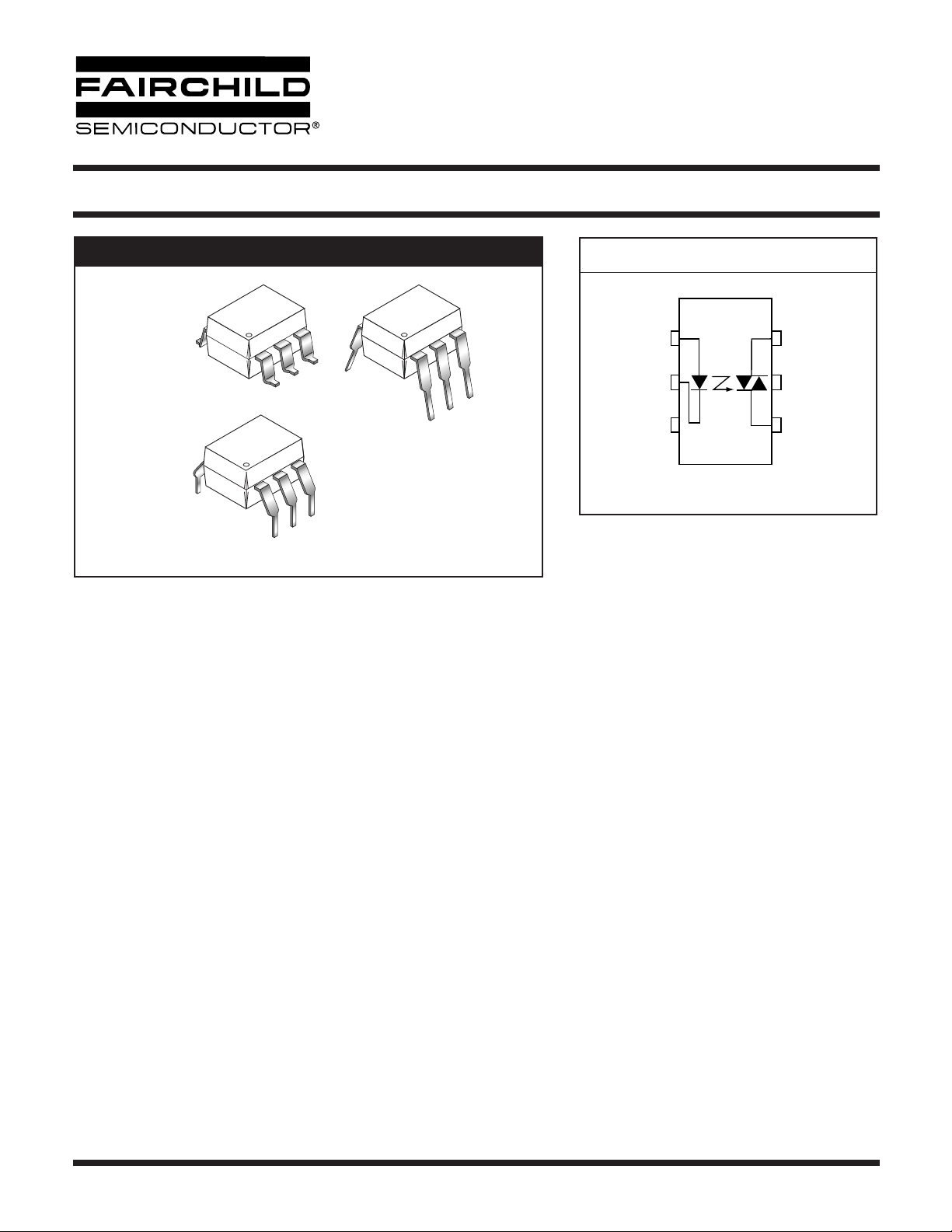
PACKAGE
SCHEMATIC
ANODE
1
MAIN TERM.
6
6
6
CATHODE
2
NC*
5
1
3
1
N/C
*DO NOT CONNECT
(TRIAC SUBSTRATE)
4
MAIN TERM.
6
1
DESCRIPTION
The MOC3051-M and MOC3052-M consist of a AlGaAs infrared emitting diode optically coupled to a non-zero-crossing silicon
bilateral AC switch (triac). These devices isolate low voltage logic from 115 and 240 Vac lines to provide random phase control of
high current triacs or thyristors. These devices feature greatly enhanced static dv/dt capability to ensure stable switching performance of inductive loads.
FEATURES
• Excellent I
• High isolation voltage—minimum 7500 peak VAC
• Underwriters Laboratory (UL) recognized—File #E90700
• 600V peak blocking voltage
• VDE recognized (File #94766)
- Ordering option V (e.g. MOC3052V-M)
stability—IR emitting diode has low degradation
FT
APPLICATIONS
• Solenoid/valve controls
• Lamp ballasts
• Static AC power switch
• Interfacing microprocessors to 115 and 240 Vac peripherals
• Solid state relay
• Incandescent lamp dimmers
•Temperature controls
• Motor controls
© 2005 Fairchild Semiconductor Corporation
Page 1 of 11
6/15/05

6-PIN DIP RANDOM-PHASE
OPTOISOLATORS TRIAC DRIVERS
(600 VOLT PEAK)
MOC3051-M MOC3052-M
ABSOLUTE MAXIMUM RATINGS
Parameters Symbol Device Value Units
TOTAL DEVICE
Storage Temperature T
Operating Temperature T
Lead Solder Temperature T
Junction Temperature Range T
(3)
Isolation Surge Voltage
Total Device Power Dissipation @ 25°C
Derate above 25°C 4.4 mW/°C
EMITTER
Continuous Forward Current I
Reverse Voltage V
Total Power Dissipation 25°C Ambient
Derate above 25°C 1.33 mW/°C
DETECTOR
Off-State Output Terminal Voltage V
Peak Repetitive Surge Current (PW = 100 ms, 120 pps) I
Total Power Dissipation @ 25°C Ambient
Derate above 25°C 4 mW/°C
(peak AC voltage, 60Hz, 1 sec duration) V
(T
= 25°C unless otherwise noted)
A
STG
OPR
SOL
J
ISO
P
D
F
R
P
D
DRM
TSM
P
D
All -40 to +150 °C
All -40 to +85 °C
All 260 for 10 sec °C
All -40 to +100 °C
All 7500 Vac(pk)
All
All 60 mA
All 3 V
All
All 600 V
All 1 A
All
330 mW
100 mW
300 mW
© 2005 Fairchild Semiconductor Corporation
Page 2 of 11
6/15/05

6-PIN DIP RANDOM-PHASE
OPTOISOLATORS TRIAC DRIVERS
(600 VOLT PEAK)
MOC3051-M MOC3052-M
ELECTRICAL CHARACTERISTICS
(T
= 25°C Unless otherwise specified)
A
INDIVIDUAL COMPONENT CHARACTERISTICS
Parameters Test Conditions Symbol Device Min Typ* Max Units
EMITTER
Input Forward Voltage I
Reverse Leakage Current V
= 10 mA V
F
= 3 V I
R
F
R
DETECTOR
Peak Blocking Current, Either Direction V
Peak On-State Voltage, Either Direction I
Critical Rate of Rise of Off-State Voltage I
TRANSFER CHARACTERISTICS
, I
= 0 (note 1) I
DRM
F
= 100 mA peak, I
TM
= 0 (figure 7, @400V) dv/dt All 1000 V/µs
F
(T
= 25°C Unless otherwise specified.)
A
= 0 V
F
DRM
TM
DC Characteristics Test Conditions Symbol Device Min Typ* Max Units
LED Trigger Current,
either direction
Main terminal
Voltage = 3V (note 2)
Holding Current, Either Direction I
*Typical values at T
= 25°C
A
I
FT
MOC3051-M 15
MOC3052-M 10
H
All 280 µA
Note
1. Test voltage must be applied within dv/dt rating.
2. All devices are guaranteed to trigger at an I
between max 15 mA for MOC3051, 10 mA for MOC3052 and absolute max I
value less than or equal to max I
F
. Therefore, recommended operating I
FT
(60 mA).
F
3. Isolation surge votlage, VISO, is an internal device breakdown rating. For this text, pins 1 and 2 are common, and pins 4, 5 and
6 are common.
All 1.15 1.5 V
All 0.05 100 µA
All 10 100 nA
All 1.7 2.5 V
mA
lies
F
© 2005 Fairchild Semiconductor Corporation
Page 3 of 11
6/15/05

0
6-PIN DIP RANDOM-PHASE
OPTOISOLATORS TRIAC DRIVERS
(600 VOLT PEAK)
MOC3051-M MOC3052-M
Figure. 1 LED Forward Voltage vs. Forward Current
1.8
1.7
1.6
1.5
1.4
1.3
- FORWARD VOLTAGE (V)
F
V
1.2
1.1
1.0
110100
IF - LED FORWARD CURRENT (mA)
Figure. 3 Trigger Current vs. Ambient Temperature
1.4
1.3
1.2
1.1
(NORMALIZED)
FT
1.0
0.9
0.8
TRIGGER CURRENT - I
0.7
NORMALIZED TO TA = 25°C
0.6
-40 -20 0 20 40 60 80 100
AMBIENT TEMPERATURE - TA (oC)
I
versus Temperature (normalized)
F
TA = -55oC
= 25oC
T
A
= 100oC
T
A
This graph (figure 3) shows the increase of the trigger current
when the device is expected to operate at an ambient temperature below 25°C. Multiply the normalized I
with the data sheet guaranteed I
FT
.
shown this graph
FT
Example:
T
= -40°C, I
A
I
@ -40°C = 10 mA x 1.4 = 14 mA
FT
= 10 mA
FT
Phase Control Considerations
LED Trigger Current versus PW (normalized)
Random Phase Triac drivers are designed to be phase controllable. They may be triggered at any phase angle within the AC
Figure. 2 On-State Characteristics
800
600
400
(mA)
TM
200
0
-200
-400
ON-STATE CURRENT - I
-600
-800
-3 -2 -1 0 1 2 3
ON-STATE VOLTAGE - VTM (V)
Figure. 4 LED Current Required to Trigger vs. LED Pulse Width
25
NORMALIZED TO:
≥
100 µs
20
15
10
5
, NORMALIZED LED TRIGGER CURRENT
FT
I
0
1
251020 50 10
PWin, LED TRIGGER PULSE WIDTH (µs)
PWin
sine wave. Phase control may be accomplished by an AC line
zero cross detector and a variable pulse delay generator which
is synchronized to the zero cross detector. The same task can
be accomplished by a microprocessor which is synchronized
to the AC zero crossing. The phase controlled trigger current
may be a very short pulse which saves energy delivered to the
input LED. LED trigger pulse currents shorter than 100 µs must
have an increased amplitude as shown on Figure 4. This graph
shows the dependency of the trigger current I
versus the
FT
pulse width can be seen on the chart delay t(d) versus the LED
trigger current.
I
in the graph I
FT
minimum specified I
the device characteristic. The normalized I
versus (PW) is normalized in respect to the
FT
for static condition, which is specified in
FT
has to be multi-
FT
plied with the devices guaranteed static trigger current.
Example:
Guaranteed I
I
(pulsed) = 10 mA x 5 = 50 mA
FT
= 10 mA, Trigger pulse width PW = 3 µs
FT
© 2005 Fairchild Semiconductor Corporation
Page 4 of 11
6/15/05
 Loading...