MOC3051M, MOC3052M — 6-Pin DIP Random-Phase Optoisolators Triac Drivers (600 Volt Peak)
September 2009
MOC3051M, MOC3052M
6-Pin DIP Random-Phase Optoisolators Triac Drivers
(600 Volt Peak)
Features
Excellent I
degradation
High isolation voltage—minimum 7500 peak VAC
Underwriters Laboratory (UL) recognized—
File #E90700, Volume 2
600V peak blocking voltage
IEC60747-5-2 approved (File #94766)
– Ordering option V (e.g. MOC3052VM)
stability—IR emitting diode has low
FT
Description
The MOC3051M and MOC3052M consist of a AlGaAs
infrared emitting diode optically coupled to a non-zerocrossing silicon bilateral AC switch (triac). These devices
isolate low voltage logic from 115 and 240 Vac lines to
provide random phase control of high current triacs or
thyristors. These devices feature greatly enhanced static
dv/dt capability to ensure stable switching performance
of inductive loads.
Applications
Solenoid/valve controls
Lamp ballasts
Static AC power switch
Interfacing microprocessors to 115 and 240 Vac
peripherals
Solid state relay
Incandescent lamp dimmers
Temperature controls
Motor controls
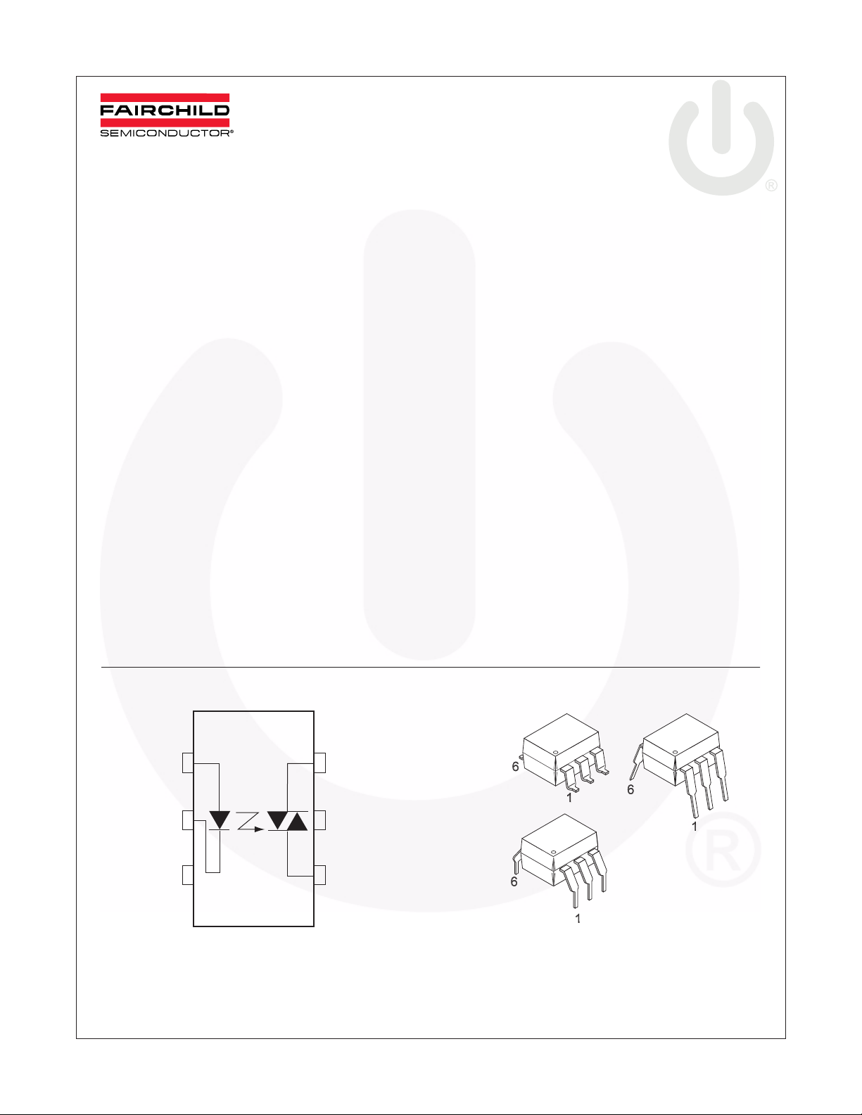
Schematic Package Outlines
ANODE
CATHODE
©2005 Fairchild Semiconductor Corporation www.fairchildsemi.com
MOC3051M, MOC3052M Rev. 1.0.5
1
2
3
N/C
*DO NOT CONNECT
(TRIAC SUBSTRATE)
MAIN TERM.
6
NC*
5
4
MAIN TERM.

MOC3051M, MOC3052M — 6-Pin DIP Random-Phase Optoisolators Triac Drivers (600 Volt Peak)
Absolute Maximum Ratings
(T
= 25°C unless otherwise specified.)
A
Stresses exceeding the absolute maximum ratings may damage the device. The device may not function or be
operable above the recommended operating conditions and stressing the parts to these levels is not recommended.
In addition, extended exposure to stresses above the recommended operating conditions may affect device reliability.
The absolute maximum ratings are stress ratings only.
Symbol Parameters Value Units
TOTAL DEVICE
T
STG
T
OPR
T
SOL
T
V
P
EMITTER
V
P
DETECTOR
V
DRM
I
TSM
P
Storage Temperature -40 to +150 °C
Operating Temperature -40 to +85 °C
Lead Solder Temperature (Wave Solder) 260 for 10 sec °C
Junction Temperature Range -40 to +100 °C
J
Isolation Surge Voltage
ISO
Total Device Power Dissipation @ 25°C
D
Derate above 25°C
Continuous Forward Current 60 mA
I
F
Reverse Voltage 3 V
R
Total Device Power Dissipation @ 25°C
D
Derate above 25°C
(1)
(peak AC voltage, 60Hz, 1 sec. duration) 7500 Vac(pk)
330 mW
4.4 mW/°C
100 mW
1.33 mW/°C
Off-State Output Terminal Voltage 600 V
Peak Repetitive Surge Current (PW = 100 µ s, 120pps) 1 A
Total Power Dissipation @ 25°C Ambient
D
Derate above 25°C
300 mW
4 mW/°C
Note:
1. Isolation surge votlage, V
ISO
and pins 4, 5 and 6 are common.
, is an internal device breakdown rating. For this text, pins 1 and 2 are common,
©2005 Fairchild Semiconductor Corporation www.fairchildsemi.com
MOC3051M, MOC3052M Rev. 1.0.5 2

Ω
MOC3051M, MOC3052M — 6-Pin DIP Random-Phase Optoisolators Triac Drivers (600 Volt Peak)
Electrical Characteristics
(T
= 25°C unless otherwise specified.)
A
Individual Component Characteristics
Symbol Parameters Test Conditions Min. Typ.* Max. Units
EMITTER
V
I
Input Forward Voltage I
F
Reverse Leakage Current V
R
= 10mA 1.18 1.5 V
F
= 3V 0.05 100 µA
R
DETECTOR
I
DRM
V
Peak Blocking Current, Either Direction V
Peak On-State Voltage, Either Direction I
TM
dv/dt Critical Rate of Rise of Off-State Voltage I
DRM
= 100mA peak, I
TM
= 0 (Figure 7, @ 400V) 1000 V/µs
F
(2)
, I
F
= 0
= 0 1.7 2.5 V
F
10 100 nA
Transfer Characteristics
Symbol DC Characteristics Test Conditions Device Min. Typ.* Max. Units
I
FT
I
H
LED Trigger Current,
Either Direction
Holding Current,
Either Direction
Main terminal
Voltage = 3V
(3)
MOC3051M 15 mA
MOC3052M 10
All 220 µA
Isolation Characteristics
Symbol Characteristic Test Conditions Min. Typ.* Max. Units
V
Input-Output Isolation
ISO
Voltage
R
Isolation Resistance V
ISO
Isolation Capacitance V = 0V, f = 1MHz 0.2 pF
C
ISO
*Typical values at T
= 25°C
A
Notes:
2. Test voltage must be applied within dv/dt rating.
3. All devices are guaranteed to trigger at an I
I
lies between max. 15A for MOC3051M, 10mA for MOC3052M and absolute max. I
F
f = 60Hz, t = 1 sec. 7500 Vac(pk)
= 500VDC 10
I-O
value less than or equal to max I
F
. Therefore, recommended operating
FT
11
(60mA).
F
©2005 Fairchild Semiconductor Corporation www.fairchildsemi.com
MOC3051M, MOC3052M Rev. 1.0.5 3

Safety and Insulation Ratings
As per IEC 60747-5-2, this optocoupler is suitable for “safe electrical insulation” only within the safety limit data.
Compliance with the safety ratings shall be ensured by means of protective circuits.
Symbol Parameter Min. Typ. Max. Unit
MOC3051M, MOC3052M — 6-Pin DIP Random-Phase Optoisolators Triac Drivers (600 Volt Peak)
Installation Classifications per DIN VDE 0110/1.89
Ta ble 1
For Rated Main Voltage < 150Vrms I-IV
For Rated Main voltage < 300Vrms I-IV
Climatic Classification 55/100/21
Pollution Degree (DIN VDE 0110/1.89) 2
CTI Comparative Tracking Index 175
V
PR
Input to Output Test Voltage, Method b,
V
x 1.875 = V
IORM
, 100% Production Test
PR
1594 V
peak
with tm = 1 sec, Partial Discharge < 5pC
Input to Output Test Voltage, Method a,
V
IORM
x 1.5 = V
, Type and Sample Test
PR
1275 V
peak
with tm = 60 sec, Partial Discharge < 5pC
V
V
IORM
IOTM
Max. Working Insulation Voltage 850 V
Highest Allowable Over Voltage 6000 V
peak
peak
External Creepage 7 mm
External Clearance 7 mm
Insulation Thickness 0.5 mm
RIO Insulation Resistance at Ts, V
= 500V 10
IO
9
Ω
©2005 Fairchild Semiconductor Corporation www.fairchildsemi.com
MOC3051M, MOC3052M Rev. 1.0.5 4
 Loading...