Fairchild MOC3042M service manual

MOC303XM, MOC304XM — 6-Pin DIP Zero-Cross Optoisolators Triac Driver Output (250/400 Volt Peak)
September 2010
MOC3031M, MOC3032M, MOC3033M,
MOC3041M, MOC3042M, MOC3043M
6-Pin DIP Zero-Cross Optoisolators Triac Driver Output
(250/400 Volt Peak)
Features
Simplifies logic control of 115 VAC power
■
■
Zero voltage crossing
dv/dt of 2000 V/µs typical, 1000 V/µs guaranteed
■
■
VDE recognized (File # 94766), ordering option V
(e.g., MOC3043VM)
Applications
Solenoid/valve controls
■
■
Lighting controls
■
Static power switches
AC motor drives
■
■
Temperature controls
E.M. contactors
■
■
AC motor starters
Solid state relays
■
Description
The MOC303XM and MOC304XM devices consist of a
GaAs infrared emitting diode optically coupled to a
monolithic silicon detector performing the function of a
zero voltage crossing bilateral triac driver.
They are designed for use with a triac in the interface of
logic systems to equipment powered from 115 VAC
lines, such as teletypewriters, CRTs, solid-state relays,
industrial controls, printers, motors, solenoids and
consumer appliances, etc.
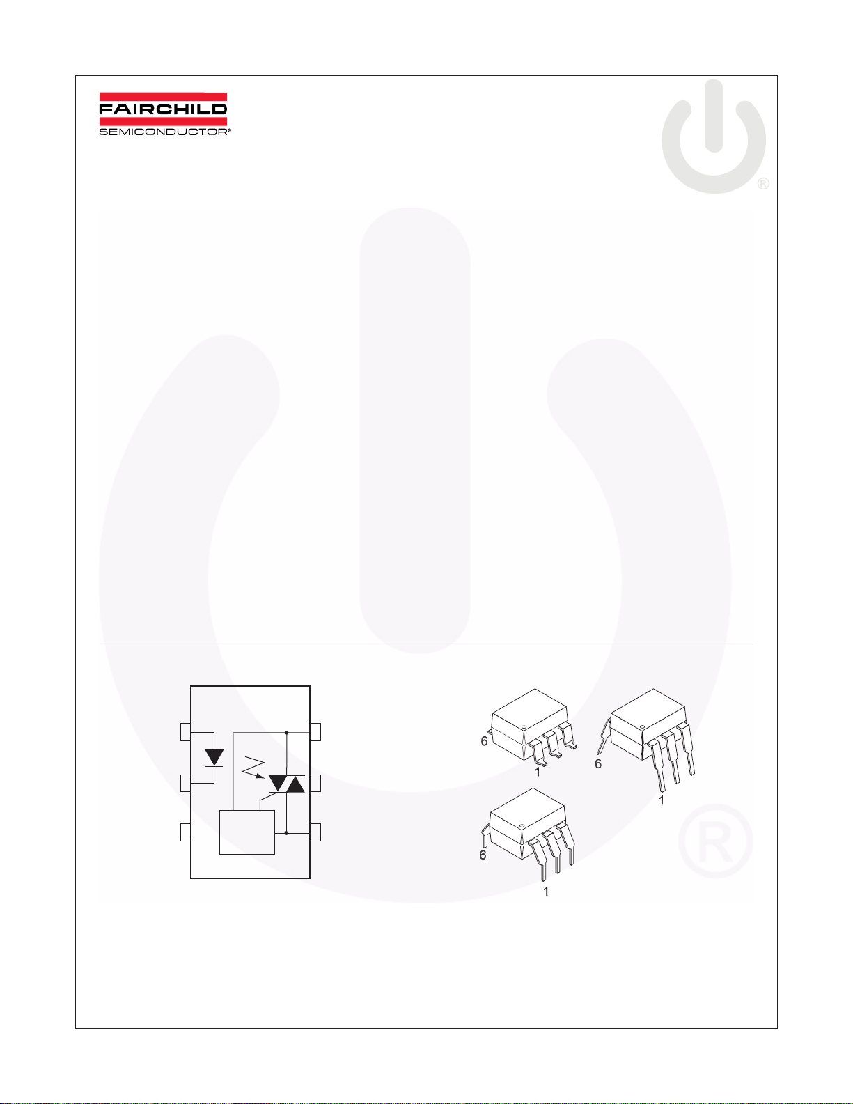
Schematic Package Outlines
N/C
1
2
3
ZERO
CROSSING
CIRCUIT
*DO NOT CONNECT
(TRIAC SUBSTRATE)
ANODE
CATHODE
©2005 Fairchild Semiconductor Corporation www.fairchildsemi.com
MOC303XM, MOC304XM Rev. 1.0.7
MAIN TERM.
6
NC*
5
4
MAIN TERM.

≤
MOC303XM, MOC304XM — 6-Pin DIP Zero-Cross Optoisolators Triac Driver Output (250/400 Volt Peak)
Absolute Maximum Ratings
(T
= 25°C unless otherwise noted)
A
Stresses exceeding the absolute maximum ratings may damage the device. The device may not function or be
operable above the recommended operating conditions and stressing the parts to these levels is not recommended.
In addition, extended exposure to stresses above the recommended operating conditions may affect device reliability.
The absolute maximum ratings are stress ratings only.
Symbol Parameters Device Value Units
TOTAL DEVICE
T
STG
T
OPR
T
SOL
T
V
ISO
P
EMITTER
I
V
P
DETECTOR
V
DRM
I
TSM
P
Storage Temperature All -40 to +150 °C
Operating Temperature All -40 to +85 °C
Lead Solder Temperature All 260 for 10
sec
Junction Temperature Range All -40 to +100 °C
J
Isolation Surge Voltage
(peak AC voltage, 60Hz, 1 sec. duration, I
Total Device Power Dissipation @ 25°C
D
Derate above 25°C
Continuous Forward Current All 60 mA
F
Reverse Voltage All 6 V
R
Total Power Dissipation 25°C Ambient
D
Derate above 25°C
(1)
2µA)
I-O
All 7500 Vac(pk)
All 250 mW
2.94 mW/°C
All 120 mW
1.41 mW/°C
Off-State Output Terminal Voltage MOC3031M/2M/3M 250 V
MOC3041M/2M/3M 400
Peak Repetitive Surge Current
All 1 A
(PW = 100µs, 120 pps)
Total Power Dissipation @ 25°C Ambient
D
Derate above 25°C
All 150 mW
All 1.76 mW/°C
°C
Note
1. Isolation surge voltage, V
, is an internal device dielectric breakdown rating. For this test, Pins 1 and 2 are
ISO
common, and Pins 4, 5 and 6 are common.
©2005 Fairchild Semiconductor Corporation www.fairchildsemi.com
MOC303XM, MOC304XM Rev. 1.0.7 2

MOC303XM, MOC304XM — 6-Pin DIP Zero-Cross Optoisolators Triac Driver Output (250/400 Volt Peak)
Electrical Characteristics
(T
= 25°C Unless otherwise specified)
A
Individual Component Characteristics
Symbol Parameters Test Conditions Device Min. Typ. Max. Units
EMITTER
V
Input Forward Voltage I
F
I
R
Reverse Leakage Current V
= 30mA All 1.25 1.5 V
F
= 6V All 0.01 100 µA
R
DETECTOR
I
DRM1
Peak Blocking Current,
Rated V
DRM
(2)
, I
F
= 0
All 100 nA
Either Direction
V
TM
Peak On-State Voltage,
I
= 100mA peak, I
TM
= 0 All 1.8 3 V
F
Either Direction
dv/dt Critical Rate of Rise of
I
= 0 (Figure 9)
F
(4)
All 1000 V/µs
Off-State Voltage
Transfer Characteristics
Symbol DC Characteristics Test Conditions Device Min. Typ. Max. Units
I
FT
I
H
LED Trigger Current Main Terminal
Voltage = 3V
Holding Current,
Either Direction
(3)
MOC3031M/
MOC3041M
MOC3032M/
15 mA
10
MOC3042M
MOC3033M/
5
MOC3043M
All 400 µA
Zero Crossing Characteristics
Symbol Characteristics Test Conditions Device Min. Typ. Max. Units
V
Inhibit Voltage I
IH
= rated I
F
, MT1-MT2
FT
voltage above which device
will not trigger
off-state
I
DRM2
Leakage in Inhibited
State
I
= rated I
F
off-state
, rated V
FT
DRM
Notes:
2. Test voltage must be applied within dv/dt rating.
3. All devices are guaranteed to trigger at an I
operating I
lies between max I
F
(15mA for MOC3031M & MOC3041M, 10mA for MOC3032M & MOC3042M,
FT
5mA for MOC3033M & MOC3043M) and absolute max I
value less than or equal to max I
F
(60mA).
F
4. This is static dv/dt. See Figure 9 for test circuit. Commutating dv/dt is a function of the load-driving thyristor(s) only.
All 20 V
All 2 mA
. Therefore, recommended
FT
©2005 Fairchild Semiconductor Corporation www.fairchildsemi.com
MOC303XM, MOC304XM Rev. 1.0.7 3

Safety and Insulation Ratings
As per IEC 60747-5-2, this optocoupler is suitable for “safe electrical insulation” only within the safety limit data.
Compliance with the safety ratings shall be ensured by means of protective circuits.
Symbol Parameter Min. Typ. Max. Unit
MOC303XM, MOC304XM — 6-Pin DIP Zero-Cross Optoisolators Triac Driver Output (250/400 Volt Peak)
Installation Classifications per DIN VDE 0110/1.89
Ta ble 1
For Rated Main Voltage < 150Vrms I-IV
For Rated Main voltage < 300Vrms I-IV
Climatic Classification 55/100/21
Pollution Degree (DIN VDE 0110/1.89) 2
CTI Comparative Tracking Index 175
V
PR
Input to Output Test Voltage, Method b,
V
x 1.875 = V
IORM
, 100% Production Test
PR
1594 V
peak
with tm = 1 sec, Partial Discharge < 5pC
Input to Output Test Voltage, Method a,
V
IORM
x 1.5 = V
, Type and Sample Test
PR
1275 V
peak
with tm = 60 sec, Partial Discharge < 5pC
V
V
IORM
IOTM
Max. Working Insulation Voltage 850 V
Highest Allowable Over Voltage 6000 V
peak
peak
External Creepage 7 mm
External Clearance 7 mm
Insulation Thickness 0.5 mm
RIO Insulation Resistance at Ts, V
= 500V 10
IO
9
Ω
©2005 Fairchild Semiconductor Corporation www.fairchildsemi.com
MOC303XM, MOC304XM Rev. 1.0.7 4
 Loading...