MOC205M, MOC206M, MOC207M, MOC208M — Small Outline Optocouplers Transistor Output
April 2009
MOC205M, MOC206M, MOC207M, MOC208M
Small Outline Optocouplers Transistor Output
Features
■
U.L. recognized (File #E90700, Volume 2)
VDE recognized (File #136616)
■
(add option “V” for VDE approval, i.e, MOC205VM)
■
Closely matched current transfer ratios
Convenient plastic SOIC-8 surface mountable
■
package style
■
Minimum BV
Standard SOIC-8 footprint, with 0.050" lead spacing
■
■
Compatible with dual wave, vapor phase and
of 70 Volts guaranteed
CEO
IR reflow soldering
High input-output isolation of 2500 V
■
AC(rms)
guaranteed
Applications
■
Feedback control circuits
Interfacing and coupling systems of different
■
potentials and impedances
■
General purpose switching circuits
Monitor and detection circuits
■
Description
These devices consist of a gallium arsenide infrared
emitting diode optically coupled to a monolithic silicon
phototransistor detector, in a surface mountable, small
outline, plastic package. They are ideally suited for high
density applications, and eliminate the need for throughthe-board mounting.
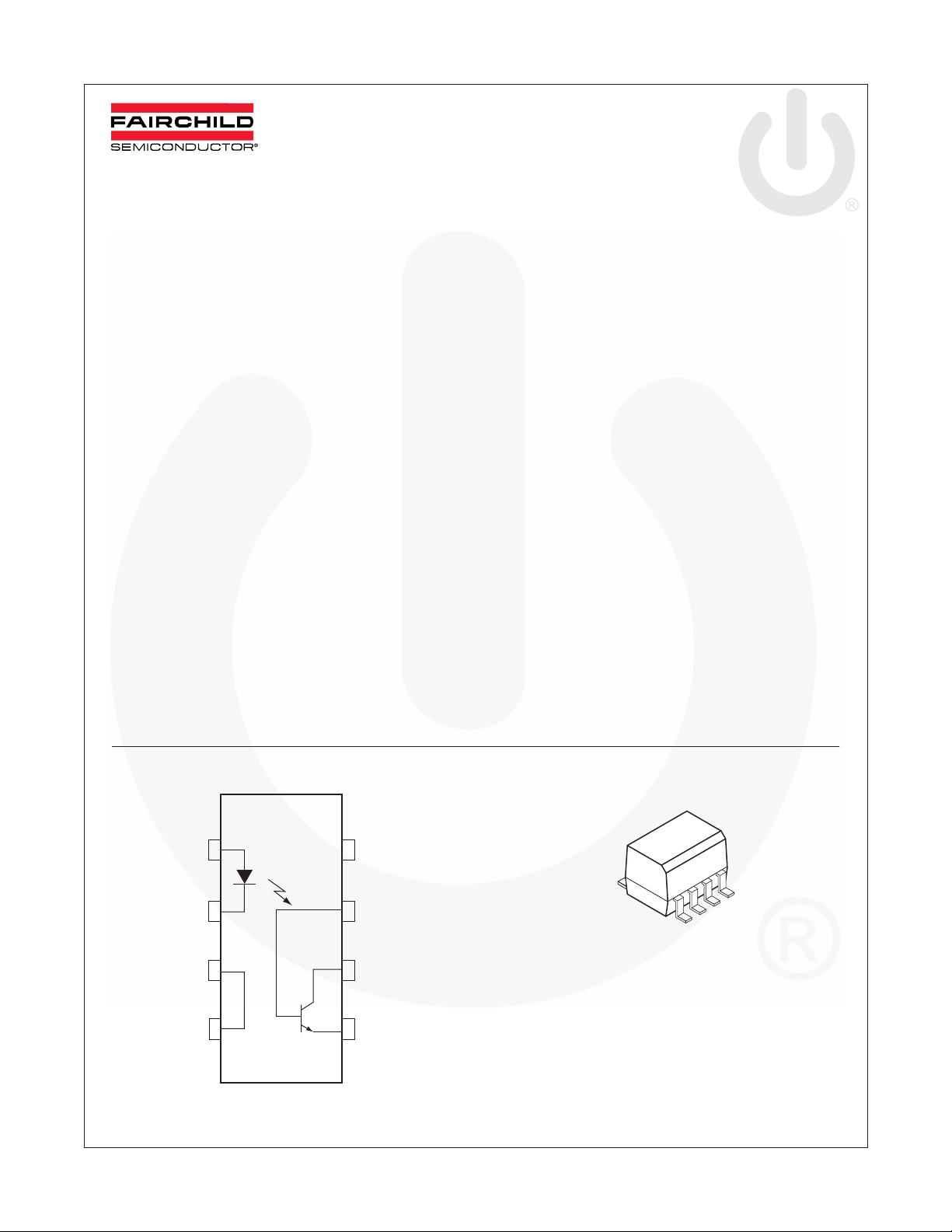
Schematic
1
N/C
2
3
4
CATHODE
©2005 Fairchild Semiconductor Corporation www.fairchildsemi.com
MOC205M, MOC206M, MOC207M, MOC208M Rev. 1.0.1
N/CANODE
8
7
BASE
COLLECTORN/C
6
EMITTER
5

MOC205M, MOC206M, MOC207M, MOC208M — Small Outline Optocouplers Transistor Output
Absolute Maximum Ratings
(T
= 25°C Unless otherwise specified)
A
Stresses exceeding the absolute maximum ratings may damage the device. The device may not function or be
operable above the recommended operating conditions and stressing the parts to these levels is not recommended.
In addition, extended exposure to stresses above the recommended operating conditions may affect device reliability.
The absolute maximum ratings are stress ratings only.
Symbol Rating Value Unit
EMITTER
I
F
I
(pk) Forward Current – Peak (PW = 100µs, 120pps) 1.0 A
F
V
R
P
D
DETECTOR
V
CEO
V
ECO
V
CBO
I
C
P
D
TOTAL DEVICE
V
ISO
P
D
T
A
T
stg
Forward Current – Continuous 60 mA
Reverse Voltage 6.0 V
LED Power Dissipation @ T
Derate above 25°C
= 25°C
A
90
0.8
mW
mW/°C
Collector-Emitter Voltage 70 V
Emitter-Collector Voltage 7.0 V
Collector-Base Voltage 70 V
Collector Current-Continuous 150 mA
Detector Power Dissipation @ T
Derate above 25°C
Input-Output Isolation Voltage (f = 60Hz, t = 1 min.)
Total Device Power Dissipation @ T
Derate above 25°C
= 25°C
A
A
= 25°C
(1)(2)(3)
150
1.76
mW
mW/°C
2500 Vac(rms)
250
2.94
mW
mW/°C
Ambient Operating Temperature Range -40 to +100 °C
Storage Temperature Range -40 to +150 °C
Notes:
1. Isolation Surge Voltage, V
, is an internal device dielectric breakdown rating.
ISO
2. For this test, Pins 1 and 2 are common and Pins 5, 6 and 7 are common.
3. V
rating of 2500 V
ISO
for t = 1 min. is equivalent to a rating of 3,000 V
AC(rms)
AC(rms)
for t = 1 sec.
©2005 Fairchild Semiconductor Corporation www.fairchildsemi.com
MOC205M, MOC206M, MOC207M, MOC208M Rev. 1.0.1 2

Ω
MOC205M, MOC206M, MOC207M, MOC208M — Small Outline Optocouplers Transistor Output
Electrical Characteristics
(T
= 25°C unless otherwise specified)
A
Symbol Parameter Test Conditions Min. Typ.* Max. Unit
EMITTER
V
Input Forward Voltage I
F
Reverse Leakage Current V
I
R
C
Input Capacitance 18 pF
IN
DETECTOR
I
CEO1
I
CEO2
BV
BV
C
Collector-Emitter Dark Current V
Collector-Emitter Breakdown Voltage I
CEO
Emitter-Collector Breakdown Voltage I
ECO
Collector-Emitter Capacitance f = 1.0 MHz, V
CE
COUPLED
CTR Collector-Output Current
MOC205M
MOC206M
MOC207M
MOC208M1
V
R
V
CE (sat)
C
*Typical values at T
Isolation Surge Voltage
ISO
Isolation Resistance
ISO
Collector-Emitter Saturation Voltage I
Isolation Capacitance
ISO
Tu r n-On Time I
t
on
Tu r n-Off Time I
t
off
Rise Time I
t
r
Fall Time I
t
f
= 25°C
A
(4)
(1)(2)(3)
(2)
(2)
= 10mA 1.15 1.5 V
F
= 6.0V 0.001 100 µA
R
= 10V, T
CE
= 10V, T
V
CE
= 100µA 70 100 V
C
= 100µA 7.0 10 V
E
= 10mA, V
I
F
= 25°C
A
= 100°C
A
= 0 7.0 pF
CE
= 10V
CE
1.0
1.0
40
63
100
40
50 nA
µA
80
125
200
125
f = 60 Hz AC Peak, t = 1 min. 2500 Vac(rms)
V = 500V 10
= 2mA, I
C
= 10mA 0.4 V
F
11
V = 0V, f = 1MHz 0.2 pF
= 2.0mA, V
C
R
= 100 Ω (Fig. 6)
L
= 2.0mA, V
C
R
= 100 Ω (Fig. 6)
L
= 2.0mA, V
C
R
= 100 Ω (Fig. 6)
L
= 2.0 mA, V
C
R
= 100 Ω (Fig. 6)
L
= 10 V,
CC
= 10V,
CC
= 10V,
CC
= 10 V,
CC
7.5 µs
5.7 µs
3.2 µs
4.7 µs
%
Notes:
1. Isolation Surge Voltage, V
, is an internal device dielectric breakdown rating.
ISO
2. For this test, Pins 1 and 2 are common and Pins 5, 6 and 7 are common.
3. V
rating of 2500 V
ISO
4. Current Transfer Ratio (CTR) = I
©2005 Fairchild Semiconductor Corporation www.fairchildsemi.com
MOC205M, MOC206M, MOC207M, MOC208M Rev. 1.0.1 3
for t = 1 min. is equivalent to a rating of 3,000 V
AC(rms)
/I
x 100%.
C
F
AC(rms)
for t = 1 sec.
