查询MM54C932供应商
MM54C932/MM74C932 Phase Comparator
General Description
The MM74C932/MM54C932 consists of two independent
output phase comparator circuits. The two phase comparators have a common signal input and a common comparator
input. The signal input can be directly coupled for a large
voltage signal, or capacitively coupled to the self-biasing
amplifier at the signal input for a small voltage signal.
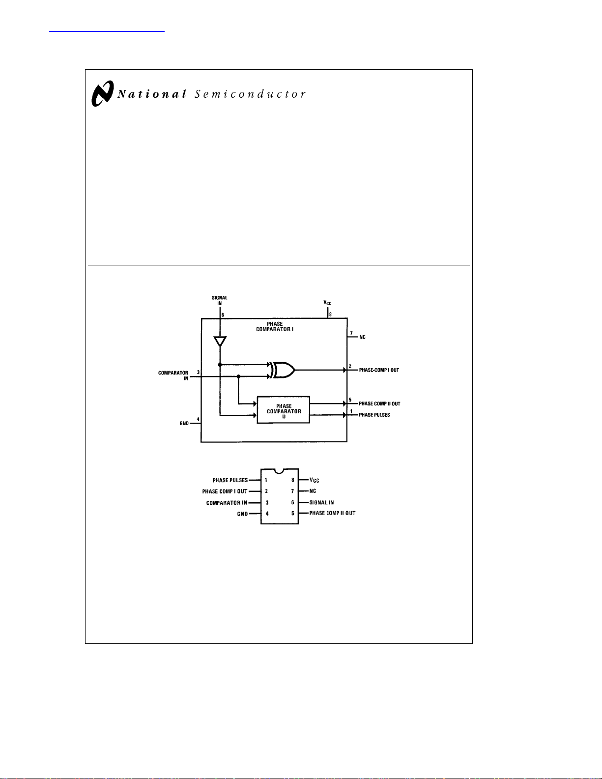
Phase comparator I, an exclusive-OR gate, provides a digital error signal (phase comp. I out) and maintains 90
shifts at the VCO center frequency. Between signal input
and comparator input (both at 50% duty cycle), it may lock
onto the signal input frequencies that are close to harmonics of the VCO center frequency.
Block and Connection Diagrams
phase
§
February 1988
Phase comparator II is an edge-controlled digital memory
network. It provides a digital error signal (phase comp. II
out) and lock in signal (phase pulses) to indicate a locked
condition and maintains a 0
put and comparator input.
phase shift between signal in-
§
Features
Y
Wide supply voltage range
Y
Convenient mini-DIP package
Y
TRI-STATEÉphase-comparator output (comparator II)
Y
200 mV input voltage (signal in) sensitivity (typical)
MM54C932/MM74C932 Phase Comparator
TL/F/5921– 1
Dual-In-Line Package
Top View
Order Number MM54C932 or MM74C932
TRI-STATEÉis a registered trademark of National Semiconductor Corporation.
C
1995 National Semiconductor Corporation RRD-B30M105/Printed in U. S. A.
TL/F/5921
TL/F/5921– 2

Absolute Maximum Ratings (Note 1)
If Military/Aerospace specified devices are required,
please contact the National Semiconductor Sales
Office/Distributors for availability and specifications.
Voltage at Any Pin
Operating Temperature Range
MM54C932
MM74C932
Storage Temperature Range
b
0.3V to V
b
b
b
a
0.3V
CC
55§Ctoa125§C
40§Ctoa85§C
65§Ctoa150§C
Power Dissipation (P
Dual-In-Line 700 mW
Small Outline 500 mW
Operating V
CC
Absolute Maximum V
Lead Temperature (Soldering, 10 seconds) 260
)
D
Range 3V to 15V
CC
18V
DC Electrical Characteristics
Symbol Parameter Conditions Min Typ Max Units
I
CC
V
OL
V
OH
V
IL
V
IH
I
OL
I
OH
I
IN
C
IN
P
D
Note 1: ‘‘Absolute Maximum Ratings’’ are those values beyond which the safety of the device cannot be guaranteed. Except for ‘‘Operating Temperature Range’’
they are not meant to imply that the devices should be operated at these limits. The table of ‘‘Electrical Characteristics’’ provides conditions for actual device
operation.
Quiescent Device Current PIN 5eVCC, PIN 8eVCC,
e
PIN 3
0V
e
V
5V 0.005 150 mA
CC
e
V
10V 0.01 300 mA
CC
e
V
15V 0.015 600 mA
CC
PIN 6eOpen, PIN 3eGND
e
V
5V 5 205 mA
CC
e
V
10V 20 710 mA
CC
e
V
15V 50 1800 mA
CC
Low Level Output Voltage V
High Level Output Voltage V
Low Level Input Voltage V
Comparator and Signal V
High Level Input Voltage V
Comparator and Signal V
Low Level Output Current V
High Level Output Current V
Input Current All Inputs except Signal Input
e
5V 0 0.05 V
CC
e
V
10V 0 0.05 V
CC
e
V
15V 0 0.05 V
CC
e
5V 4.95 5 V
CC
e
V
10V 9.95 10 V
CC
e
V
15V 14.95 15 V
CC
e
CC
e
CC
e
V
CC
e
CC
e
CC
e
V
CC
e
CC
e
V
CC
e
V
CC
e
CC
e
V
CC
e
V
CC
e
V
CC
e
V
CC
5V, V
10V, V
15V, V
5V, V
10V, V
15V, V
5V, V
10V, V
15V, V
5V, V
10V, V
15V, V
15V, V
15V, V
e
0.5V or 4.5V 1.5 V
O
e
1V or 9V 3.0 V
O
e
1.5V or 13.5V 4.0 V
O
e
0.5V or 4.5V 3.5 V
O
e
1V or 9V 7.0 V
O
e
1.5V or 13.5V 11.0 V
O
e
0.4V 0.36 0.88 mA
O
e
0.5V 0.9 2.25 mA
O
e
1.5V 2.4 8.8 mA
O
e
4.6V
O
e
9.5V
O
e
13.5V
O
e
0V
IN
e
15V 10
IN
b
0.36
b
0.9
b
2.4
b
0.88 mA
b
2.25 mA
b
8.8 mA
b
5
b
10
b
5
b
1.0 mA
1.0 mA
Input Capacitance Any Input 7.5 pF
Total Power Dissipation f
e
10 kHz, R1e1MX
o
R2
V
V
V
CC
CC
CC
e %
e
e
e
e
, VCO
5V 0.07 mW
VCC/2
IN
10V 0.6 mW
15V 2.4 mW
C
§
2
 Loading...