

Fairchild ML6426 service manual
查询ML6426-1供应商
www.fairchildsemi.com
ML6426
High Bandwidth Triple Video Filters with Buffered
Outputs for RGB or YUV
Features
• 5V ±10% operation
• RGB/YUV filters for ATSC Digital Television VESA
Standard
• 2:1 Mux Inputs for multiple RGB/YUV inputs
• Triple Reconstruction Filter options for 6.7, 12, 24, 30,
and 36MHz to handle various line rates
• Multiple ML6426 outputs can be paralleled to drive RGB/
YUV outputs at different frequencies for various line rates
by means of Disable/Enable pin.
• 6dB drivers and sync tip clamps for DC restore
• DC restore with minimal tilt
• 0.4% differential gain on all channels
0.4º differential phase on all channels
0.8% total harmonic distortion on all channels
• 2kV ESD protection
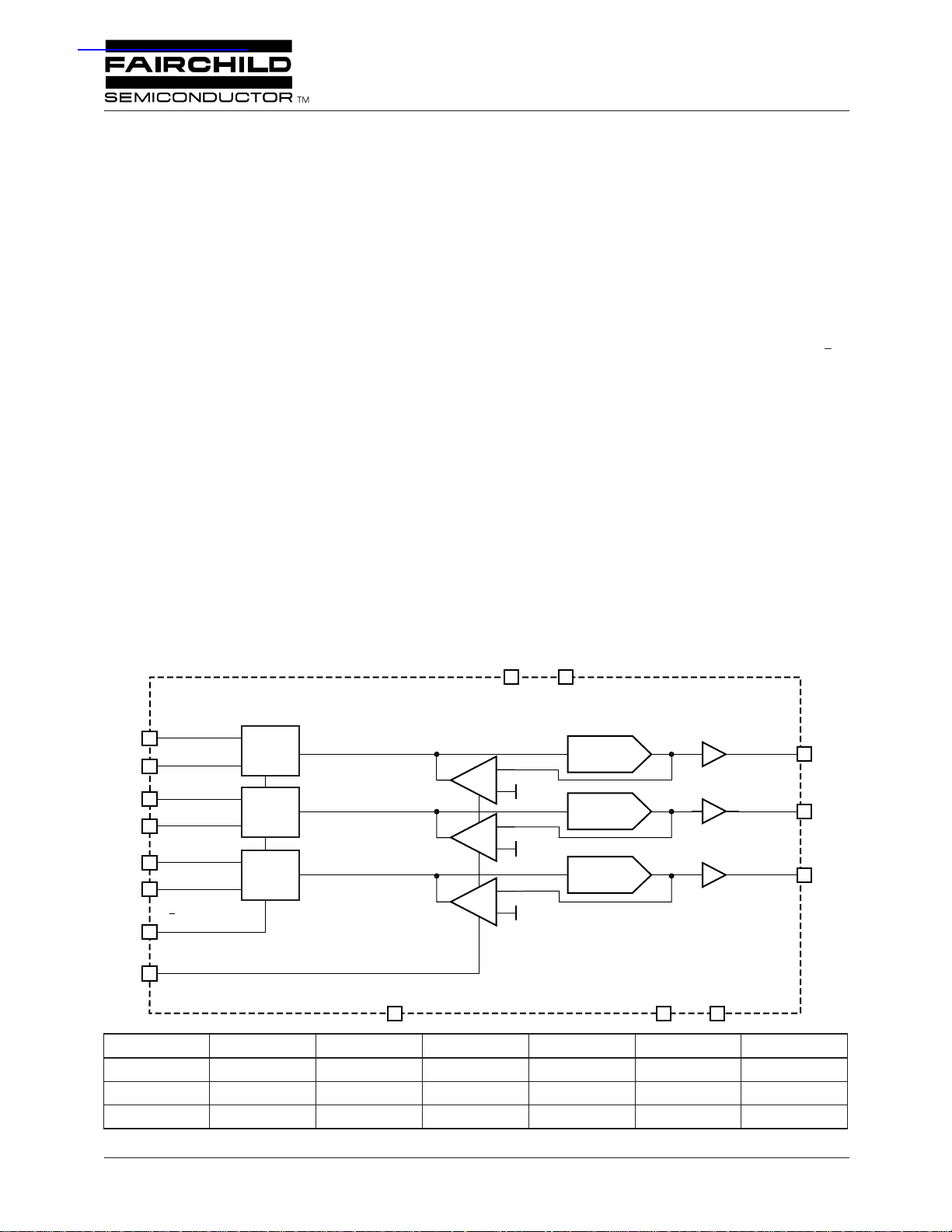
Block Diagram
RINA/YINA
2
RINB/YINB
5
GINA/UINA
6
GIN/UINB
7
BINA/VINA
8
BINB/VINB
9
A/B MUX
1
MUX
TRANSCONDUCTANCE
ERROR AMP
MUX
TRANSCONDUCTANCE
ERROR AMP
MUX
TRANSCONDUCTANCE
ERROR AMP
General Description
The ML6426 are a family of triple video filters with buffered
outputs. There are several versions of the ML6426, each with
different passband cut-off frequencies of 6.7MHz, 12MHz,
24MHz, 30MHz, and 36MHz. Each channel contains a 4
order Butterworth lowpass reconstruction video filter. The
filter is optimized for minimum overshoot and flat group
delay and guaranteed differential gain and phase at the outputs of the integrated cable drivers.
All input signals from DACs are AC coupled into the
ML6426. All channels have DC restore circuitry to clamp the
DC input levels during video H-sync, using an output feedback clamp. An external H-sync signal is required for this
purpose.
All outputs must be AC coupled into their loads. Each output
can drive 2V
2 (6dB) at 1V
12
V
CCO
+
–
0.5V
+
–
0.5V
+
–
0.5V
into a 150 Ω load. All channels have a gain of
P-P
input levels.
P-P
4
V
CC
R
4th-ORDER
FILTER A
4th-ORDER
FILTER B
4th-ORDER
FILTER C
×2
×2
×2
OUT/YOUT
G
OUT/UOUT
B
OUT/VOUT
th
-
13
11
10
SYNCIN
16
DISABLE
15
GNDO
14
GND
3
ML6426-1 ML6426-2 ML6426-3 ML6426-4 ML6426-5 ML6426-15
Filter A 6.7MHz 12MHz 24MHz 30MHz 36MHz 15MHz
Filter B 6.7MHz 12MHz 24MHz 30MHz 36MHz 15MHz
Filter C 6.7MHz 12MHz 24MHz 30MHz 36MHz 15MHz
REV. 3A August 2004
A
B
A
B
A
B
ML6426 DATA SHEET
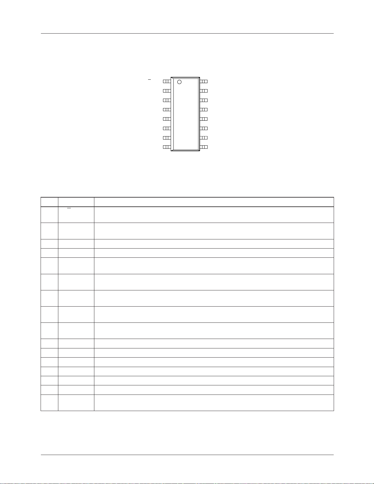
Pin Configuration
ML6426
16-Pin Narrow SOIC (S16N)
16
A/B MUX
RINA/YINA
GND
V
CC
RINB/YINB
GINA/UINA
GINB/UINB
BINA/VINA
1
2
3
4
5
6
7
8
TOP VIEW
SYNC IN
15
DISABLE
14
GNDO
13
R
OUT/YOUT
12
V
CCO
11
G
OUT/UOUT
10
B
OUT/VOUT
9
BINB/VINB
Pin Description
PIN NAME FUNCTION
1 A/B MUX Logic input pin to select between Bank <A> and Bank <B> video inputs . This pin is
internally pulled high.
2R
3 GND
4V
5R
6G
7G
8B
9B
10 B
11 G
12 V
13 R
14 GNDO
15 DISABLE Disable/Enable pin . Turns the chip off when logic high. Internally pulled low.
16 SYNC IN
A/Y
IN
CC
B/Y
IN
A/U
IN
B/U
IN
A/V
IN
B/V
IN
OUT
OUT
CCO
OUT
Unfiltered analog R- or Y-channel input for Bank <A> . Sync must be provided at
IN
SYNC IN pin.
Analog ground
Analog 5V supply
Unfiltered analog R- or Y-channel input for Bank <B> . Sync must be provided at
IN
SYNC IN pin.
Unfiltered analog G- or U-channel input for Bank <A> . Sync must be provided at
IN
SYNC IN pin.
Unfiltered analog G- or U-channel input for Bank <B> . Sync must be provided at
IN
SYNC IN pin.
Unfiltered analog B- or V-channel input for Bank <A> . Sync must be provided at
IN
SYNC IN pin.
Unfiltered analog B- or V-channel input for Bank <B> . Sync must be provided at
IN
SYNC IN pin.
Analog B or V-channel output
Analog G or U-channel output
5V power supply for output buffers
Analog R or Y-channel output
Analog ground
Input for an external H-sync logic signal for filter channels . CMOS level input.
Active High.
2
REV. 3A August 2004
DATA SHEET ML6426
Absolute Maximum Ratings
Absolute maximum ratings are those values beyond which the device could be permanently damaged. Absolute maximum
ratings are stress ratings only and functional device operation is not implied.
Parameter Min. Max. Unit
V
CC
–0.3 7 V
Junction Temperature 150 °C
ESD >2000 V
Analog and Digital I/O GND – 0.3 V
+ 0.3 V
CC
Storage Temperature Range –65 150 °C
Lead Temperature (Soldering, 10 sec) 260 °C
Thermal Resistance ( θ
) 100 °C/W
JA
Operating Conditions
Parameter Min. Max. Unit
Temperature Range 0 70 °C
V
Range 4.5 5.5 V
CC
Electrical Characteristics
Unless otherwise specified, V
Symbol Parameter Conditions Min Typ Max Units
General
I
A
V
CC
V
OUT
Supply Current No Load (V
Low Frequency Gain (R, G, B) V
Output Level during Sync (R, G, B,)
Output Capability
t
CLAMP
V
I
Clamp Response Time Settled to Within 10mV,
Input Signal Dynamic Range (R, G, B,) AC Coupled 1.4 V
OS Peak Overshoot (R, G, B,) 2V
C
L
Output Load Capacitance (R, G, B,) All Outputs 35 pF
Output Load Drive Capability, per Pin
(YUV or RGB Outputs)
dG Differential Gain (R, G, B,) All Outputs at f
d φ
T
HD
Differential Phase (R, G, B,) All Outputs at f
Output Distortion (R, G, B,) V
PSRR PSRR (R, G, B,) 0.5V
I
SC
V
V
T
MUX
IH
IL
Output Short Circuit Current (R, G, B,) Note 2 120 mA
Input Voltage Logic High DISABLE, SYNC IN 2.5 V
Input Voltage Logic Low DISABLE, SYNC IN 1.0 V
Input Mux
Data Valid
Time
= 5V±10%, T
CC
= Operating Temperature Range (Note 1)
A
= 5.5V) 52 80 mA
CC
= 100mV
IN
at 100KHz 5.34 6.0 6.65 dB
P-P
DURING SYNC 0.7 0.9 1.2 V
RL = 150 Ω , AC-coupled@1MHz 2 V
10 ms
C
= 0.1µF
IN
Output Pulse 4.3 %
P-P
One Load is 150 Ω
C
C
OUT
= 2V
P-P
at 1 MHz 0.8 %
P-P
(100kHz) at V
A/B Mux
/2 0.4 %
/2 0.4 °
CC
2 loads
35 dB
2µs
Pin Valid
High or Low
P-P
P-P
REV. 3A August 2004
3
≥
ML6426 DATA SHEET
Electrical Characteristics (continued)
Unless otherwise specified, V
Symbol Parameter Conditions Min Typ Max Units
6.7MHz Filter: ML6426-1
f
1dB
f
c
f
0.8fc
f
SB
–1dB Bandwidth Flatness (R, G, B,) 25°C 4.0 4.8 MHz
–3dB Bandwidth Flatness (R, G, B,) 25°C 6.0 6.7 MHz
0.8 x f
Attenuation 1.5 dB
C
StopBand Rejection
(All Channels ≥ 4 f
NOISE Output Noise (R, G, B,) Fullband 1.0 mV
X
TALK
X
TALK
T
PD
T
PD
Crosstalk Input of 0.5V
A/B MUX Crosstalk Input of 0.5V
Group Delay (R, G, B,) 100kHz 70 ns
Group Delay Deviation from Flatness
(R, G, B,)
12MHz Filter: ML6426-2
f
1dB
f
c
f
0.8fc
f
SB
–1dB Bandwidth Flatness (R, G, B,) 25°C 7.8 9.2 MHz
–3dB Bandwidth Flatness (R, G, B,) 25°C 10.8 12 MHz
0.8 x f
Attenuation 1.2 dB
C
StopBand Rejection
(All Channels ≥ 4 f
NOISE Output Noise (R, G, B,) Fullband 1 mV
X
TALK
X
TALK
T
PD
∆T
PD
Crosstalk Input of 0.5V
A/B MUX Crosstalk Input of 0.5V
Group Delay (R, G, B,) 100kHz 40 ns
Group Delay Deviation from Flatness
(R, G, B,)
24MHz Filter: ML6426-3
f
1dB
f
c
f
0.8fc
f
SB
–1dB Bandwidth Flatness (R, G, B,) 25°C 13.6 16 MHz
–3dB Bandwidth Flatness (R, G, B,) 25°C 21.6 24 MHz
0.8 x fC Attenuation 1.7 dB
StopBand Rejection
(All Channels ≥ 4 fC)
NOISE Output Noise (R, G, B,) Fullband 1.0 mV
X
TALK
X
TALK
T
PD
∆T
PD
Crosstalk Input of 0.5V
A/B MUX Crosstalk Input of 0.5V
Group Delay (R, G, B,) 100kHz 22 ns
Group Delay Deviation from Flatness
(R, G, B,)
= 5V±10%, TA = Operating Temperature Range (Note 1)
CC
f
4 fC, Note 3 –38 –42 dB
IN
)
C
at 1 MHz
P-P
Between any two Channels
at 3.58/4.43MHz –54 dB
P-P
to 3.58MHz 4.0 ns
to 4.43MHz 8.0 ns
to 10MHz 9 ns
f
≥ 4 fC, Note 3 –40 dB
IN
)
C
at 1 MHz
P-P
Between any two Channels
at 3.58/4.43MHz –54 dB
P-P
to 3.58MHz 1 ns
to 4.43MHz 1 ns
to 10MHz 7 ns
fIN ≥ 4 fC, Note 3 –40 dB
at 1 MHz
P-P
Between any two Channels
at 3.58/4.43MHz -54 dB
P-P
to 3.58MHz 1 ns
to 4.43MHz 1 ns
to 10MHz 2 ns
RMS
–55 dB
RMS
–55 dB
RMS
–55 dB
∆
4
REV. 3A August 2004
DATA SHEET ML6426
Electrical Characteristics (continued)
Unless otherwise specified, V
Symbol Parameter Conditions Min Typ Max Units
30MHz Filter: ML6426-4
f
1dB
f
c
f
0.8fc
f
SB
–1dB Bandwidth Flatness (R, G, B,) 25°C 15.3 18 MHz
–3dB Bandwidth Flatness (R, G, B,) 25°C 27 30 MHz
0.8 x fC Attenuation 1.7 dB
StopBand Rejection
(All Channels ≥ 4 f
NOISE Output Noise (R, G, B,) Fullband 1.0 mV
X
TALK
X
TALK
T
PD
∆T
PD
Crosstalk Input of 0.5V
A/B MUX Crosstalk Input of 0.5V
Group Delay (R, G, B,) 100kHz 18 ns
Group Delay Deviation from Flatness
(R, G, B,)
36MHz Filter: ML6426-5
f
1dB
f
c
f
0.8fc
f
SB
–1dB Bandwidth Flatness (R, G, B,) 25°C 17 20 MHz
–3dB Bandwidth Flatness (R, G, B,) 25°C 32.4 36 MHz
0.8 x fC Attenuation 2 dB
StopBand Rejection
(All Channels ≥ 4 fC)
NOISE Output Noise (R, G, B,) Fullband 1.0 mV
X
TALK
X
TALK
T
PD
∆T
PD
Crosstalk Input of 0.5V
A/B MUX Crosstalk Input of 0.5V
Group Delay (R, G, B,) 100kHz 17 ns
Group Delay Deviation from Flatness
(R, G, B,)
15MHz Filter: ML6426-15
f
1dB
f
c
f
0.8fc
f
SB
–1dB Bandwidth Flatness (R, G, B,) 25°C 10.8 12.2 MHz
–3dB Bandwidth Flatness (R, G, B,) 25°C 13.8 15 MHz
0.8 x fC Attenuation 1.2 dB
StopBand Rejection (All Channels ≥ 4 fC)
NOISE Output Noise (R, G, B,) Fullband 1.0 mV
X
TALK
X
TALK
T
PD
∆T
PD
Crosstalk Input of 0.5V
A/B MUX Crosstalk Input of 0.5V
Group Delay (R, G, B,) 100kHz 40 ns
Group Delay Deviation from Flatness
(R, G, B,)
Notes
1. Limits are guaranteed by 100% testing, sampling, or correlation with worst case test conditions.
2. Sustained short circuit protection limited to 10 seconds.
3. 38dB is based on tester noise limits.
= 5V±10%, TA = Operating Temperature Range (Note 1)
CC
≥ 4 fC, Note 3 -40 dB
f
IN
)
C
at 1 MHz
P-P
Between any two Channels
at 3.58/4.43MHz -54 dB
P-P
to 10MHz 0.5 ns
to 27MHz 2 ns
fIN ≥ 4 fC, Note 3 –40 dB
at 1 MHz
P-P
Between any two Channels
at 3.58/4.43MHz –54 dB
P-P
to 10MHz 0.5 ns
to 30MHz 4 ns
fIN ≥ 4 fC, Note 3 –40 dB
at 1 MHz
P-P
Between any two Channels
at 3.58/4.43MHz –54 dB
P-P
to 3.58MHz 1 ns
to 4.43MHz 1 ns
to 10MHz 9 ns
RMS
-55 dB
RMS
–55 dB
RMS
–55 dB
REV. 3A August 2004 5
ML6426 DATA SHEET
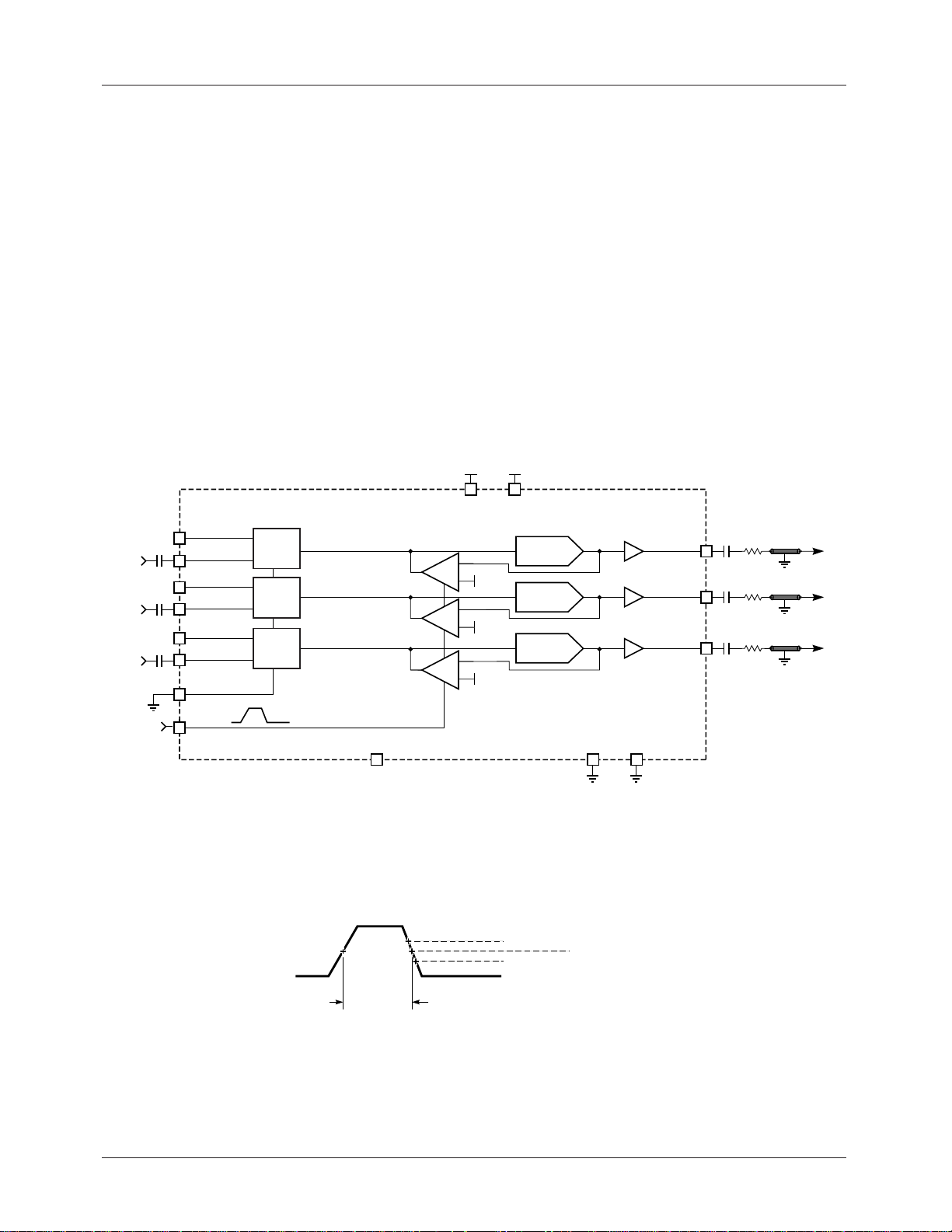
Functional Description
The ML6426 is a triple monolithic continuous time video
filter designed for reconstructing video signals from an
YUV/RGB video D/A source. The ML6426 is intended for
use in AC coupled input and output applications.
The filters approximate a 4th-order Butterworth characteristic with an optimization toward low overshoot and flat group
delay. All outputs are capable of driving 2V
coupled 150Ω video loads, with up to 35pF of load capacitance. All outputs are capable of driving a 75Ω load at 1V
All channels are clamped during sync to establish the appropriate output voltage swing range (DC restore). Thus the
input coupling capacitors do not behave according to the
RINA/YINA
2
R
IN
G
IN
B
IN
SYNC IN
0.1µF
0.1µF
0.1µF
RINB/YINB
5
GINA/UINA
6
GINB/UINB
7
BINA/VINA
8
BINB/VINB
9
A/B MUX
1
SYNCIN
16
MUX
TRANSCONDUCTANCE
MUX
TRANSCONDUCTANCE
MUX
TRANSCONDUCTANCE
ACTIVE HIGH
into AC
P-P
ERROR AMP
ERROR AMP
ERROR AMP
DISABLE
15
P-P
conventional RC time constant. In most applications, the
ML6426's input coupling capacitors are only 0.1µF.
An external CMOS compatible HSYNC pulse is required
which is Active High on the SYNC IN Pin. See Figure 2.
During sync, the feedback clamp sources/sinks current to
restore the DC level. The net result is that the average input
current is zero. Any change in the input coupling capacitors'
value will linearly affect the clamp response times.
Each channel is essentially tilt-free. Each input is clamped
.
by a feedback amp which responds to the output during sync.
The ML6426 is robust and stable under all stated load and
input conditions. Bypassing both V
pins directly to
CC
ground ensures this performance.
5V 5V
12
0.5V
0.5V
0.5V
4
V
CC
4th-ORDER
FILTER A
4th-ORDER
FILTER B
4th-ORDER
FILTER C
GNDO
14
×2
×2
×2
GND
R
G
B
3
OUT/YOUT
OUT/UOUT
OUT/VOUT
220µF
75Ω
13
220µF
75Ω
11
220µF
75Ω
10
V
CCO
+
–
+
–
+
–
R
G
B
Figure 1. Typical Application Schematic
V
= 2.5V
PW
MIN
IH
VIL = 1.0V
= 2µS
50% x V
SYNC IN
Figure 2. SYNC IN Pulse Width
6 REV. 3A August 2004
 Loading...