

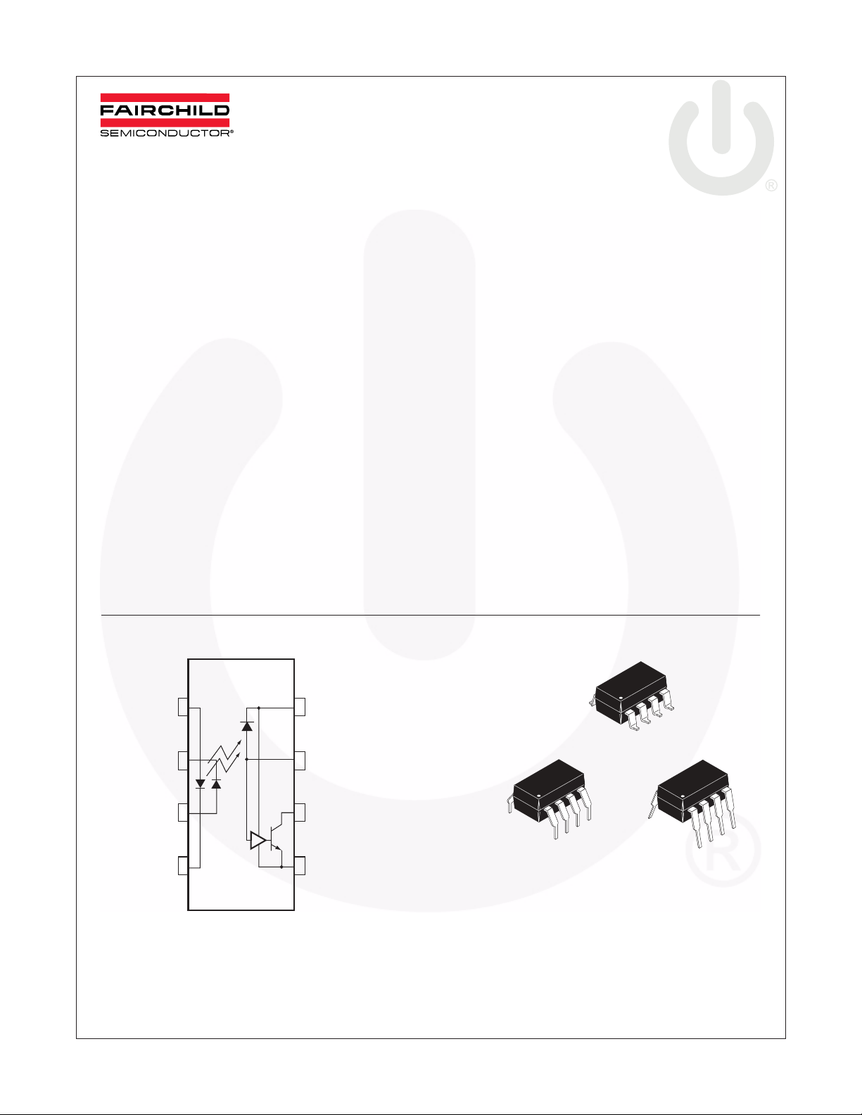
MID400 — AC Line Monitor Logic-Out Device
April 2010
MID400
AC Line Monitor Logic-Out Device
Features
■
Direct operation from any line voltage with the use of
an external resistor.
■
Externally adjustable time delay
■
Externally adjustable AC voltage sensing level
High voltage isolation between input and output
■
■
Compact plastic DIP package
Logic level compatibility
■
■
UL recognized (File #E90700)
VDE recognized (file #102915), – add option V
■
(e.g., MID400V)
Description
The MID400 is an optically isolated AC line-to-logic interface device. It is packaged in an 8-lead plastic DIP. The
AC line voltage is monitored by two back-to-back GaAs
LED diodes in series with an external resistor. A high
gain detector circuit senses the LED current and drives
the output gate to a logic low condition.
The MID400 has been designed solely for the use as an
AC line monitor
AC-to-DC control application where excellent optical isolation, solid state reliability, TTL compatibility, small size,
low power, and low frequency operations are required.
. It is recommended for use in any
Applications
■
Monitoring of the AC/DC “line-down” condition
“Closed-loop” interface between electromechanical
■
elements such as solenoids, relay contacts, small
motors, and microprocessors
■
Time delay isolation switch
Schematic Package Outlines
1
N/C
2
3
N/C
4 5
8
7
6
V
CC
AUX
V
0
GND
8
1
8
1
8
1
Equivalent Circuit
©2005 Fairchild Semiconductor Corporation www.fairchildsemi.com
MID400 Rev. 1.0.4
MID400 — AC Line Monitor Logic-Out Device
Absolute Maximum Ratings
Stresses exceeding the absolute maximum ratings may damage the device. The device may not function or be
operable above the recommended operating conditions and stressing the parts to these levels is not recommended.
In addition, extended exposure to stresses above the recommended operating conditions may affect device reliability.
The absolute maximum ratings are stress ratings only.
Symbol Parameter Value Unit
TOTAL DEVICE
T
STG
T
OPR
T
SOL
P
Total Device Power Dissipation @ T
D
EMITTER
LED Power Dissipation @ T
P
D
DETECTOR
I
OL
V
OH
V
CC
P
D
Storage Temperature -55 to +125 °C
Operating Temperature -40 to +85 °C
Lead Solder Temperature 260 for 10 sec °C
= 25°C 115 mW
A
Derate above 70°C 4.0 mW/°C
Steady State Isolation 2500 VRMS
RMS Current 25 mA
DC Current ±30 mA
= 25°C 45 mW
A
Derate above 70°C 2.0 mW/°C
Low Level Output Current 20 mA
High Level Output Voltage 7.0 V
Supply Voltage 7.0 V
Detector Power Dissipation @ T
= 25°C 70 mW
A
Derate above 70°C 2.0 mW/°C
©2005 Fairchild Semiconductor Corporation www.fairchildsemi.com
MID400 Rev. 1.0.4 2
≤
≤
≤
Ω
MID400 — AC Line Monitor Logic-Out Device
Electrical Characteristics
(0°C to 70°C Free Air Temperature unless otherwise specified-All typical values are at 25°C)
Individual Component Characteristics
Symbol Parameter Test Conditions Min. Typ. Max. Unit
EMITTER
V
Input Forward Voltage I
F
= ±30 mA, DC 1.5 V
F
DETECTOR
I
CCL
Logic Low Output Supply
Current
I
= 4.0 mA RMS,
IN
V
= Open, V
O
= 5.5V, 24V V
CC
I (ON)
3.0 mA
,
RMS ≤ 240V
I
CCH
Logic High Output
Supply Current
I
= 0.15mA RMS, V
IN
V
, RMS ≥ 5.5V
I (OFF)
= 5.5V,
CC
0.80 mA
Transfer Characteristics
Symbol DC Characteristics Test Conditions Min. Typ. Max. Units
V
OL
I
OH
V
RMS On-state RMS Input
I (ON)
V
I (OFF)
I
RMS On-state RMS
I (ON)
I
RMS Off-state RMS Input
I (OFF)
Logic Low Output
Current
Logic High Output
Current
Voltage
RMS Off-state RMS Input
Voltage
Input Current
Current
I
= I
IN
24V ≤ V
I
= 0.15mA RMS, V
IN
V
I (OFF)
V
= 0.4V, I
O
R
IN
V
= V
O
R
IN
V
= 0.4V, I
O
24V ≤ V
V
= V
O
RMS, I
I (ON)
I (ON)
, RMS ≥ 5.5V
= 22k Ω
= 5.5 V, I
CC
= 22k Ω
I (ON)
= 5.5V, I
CC
, RMS ≤ 240V
= 16mA, V
O
= 16mA, V
O
, RMS ≤ 240V
RMS ≥ 5.5V
= 16mA, V
O
= V
O
CC
100µA,
O
CC
100µA, V
O
CC
= 5.5V,
CC
= 4.5V,
= 4.5V,
I (OFF)
= 4.5V,
,
0.18 0.40 V
0.02 100 µA
90 V
5.5 V
4.0 mA
0.15 mA
Transfer Characteristics
Symbol Characteristics Test Conditions Min. Typ. Max. Units
SWITCHING TIME (T
t
t
OFF
ON
Tu r n-On Time I
Tu r n-Off Time I
(RMS = True RMS Voltage at 60 Hz, THD ≤ 1%)
Isolation Characteristics
= 25°C)
A
(T
= 25°C)
A
= 4.0mA RMS, I
IN
V
= 4.5V, R
CC
= 22k Ω
IN
(See Test Circuit 2)
= 4.0mA RMS, I
IN
V
= 4.5V, R
CC
= 22k Ω
IN
(See Test Circuit 2)
= 16mA,
O
= 16mA,
O
1.0 ms
1.0 ms
Symbol Characteristics Test Conditions Min. Typ. Max. Units
V
R
C
©2005 Fairchild Semiconductor Corporation www.fairchildsemi.com
MID400 Rev. 1.0.4 3
Steady State Isolation
ISO
Voltage
Isolation Resistance V
ISO
Isolation Capacitance f = 1MHz 2 pF
ISO
Relative Humidity ≤ 50%,
I
10µA, 1 Minute, 60Hz
I-O
= 500VDC 10
I-O
2500 VRMS
11
MID400 — AC Line Monitor Logic-Out Device
Description/Applications
The input of the MID400 consists of two back-to-back
LED diodes which will accept and convert alternating
currents into light energy. An integrated photo diodedetector amplifier forms the output network. Optical coupling between input and output provides 2500 VRMS
voltage isolation. A very high current transfer ratio
(defined as the ratio of the DC output current and the DC
input current) is achieved through the use of high gain
amplifier. The detector amplifier circuitry operates from a
5V DC supply and drives an open collector transistor
output. The switching times are intentionally designed to
be slow in order to enable the MID400, when used as an
AC line monitor, to respond only to changes in input voltage exceeding many milliseconds. The short period of
time during zero-crossing which occurs once every half
cycle of the power line is completely ignored. To operate
the MID400, always add a resistor, R
, in series with the
IN
input (as shown in test circuit 1) to limit the current to the
required value. The value of the resistor can be determined by the following equation:
VINVF–
R
=
-----------------------
IN
Where,
V
(RMS) is the input voltage.
IN
is the forward voltage drop across the LED.
V
F
IIN (RMS) is the desired input current required to sustain a logic
“O” on the output.
I
IN
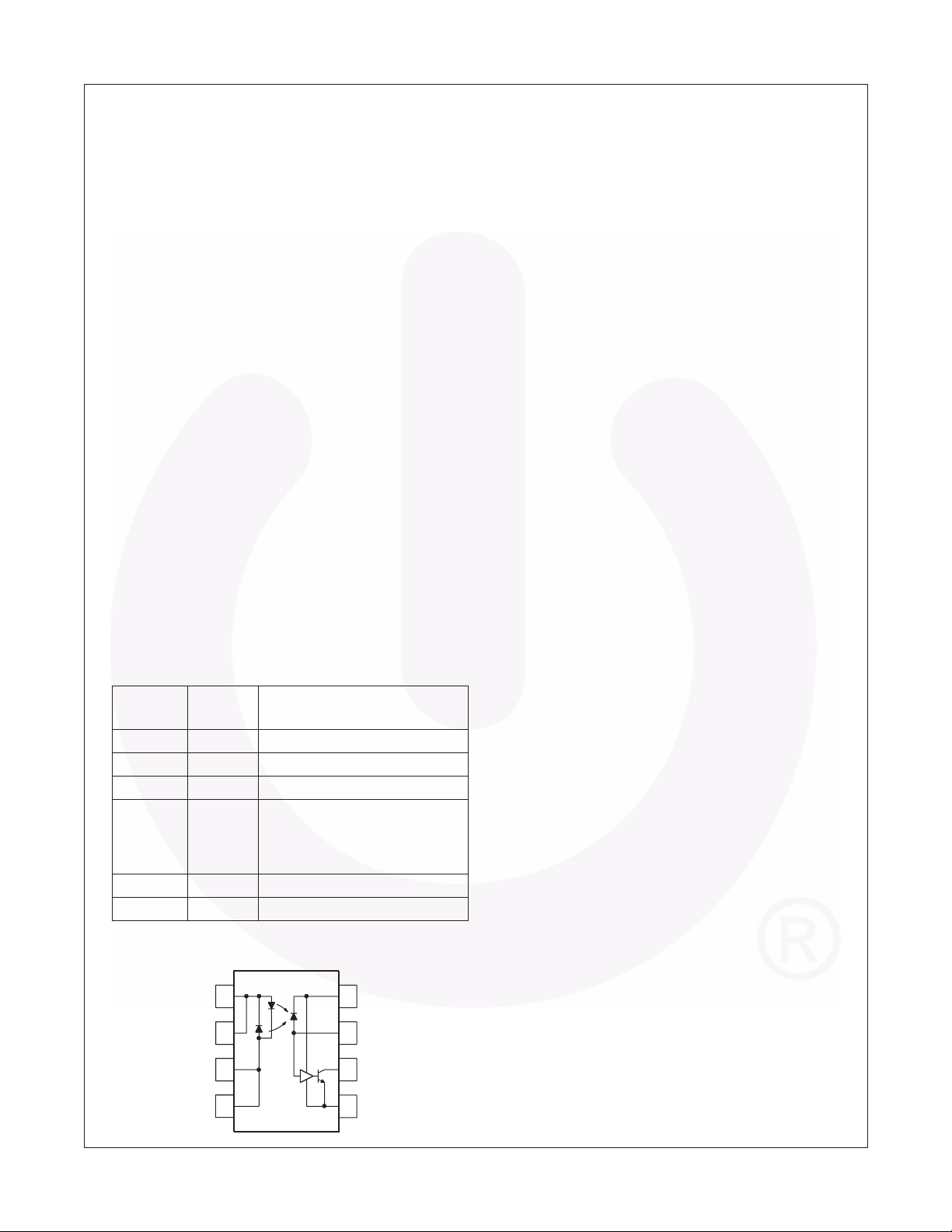
Pin Description
Pin
Number
1, 3 V
2, 4 N/C No Connect
8V
7AUX Auxiliary terminal.
6VOOutput terminal; open collector.
5 GND Circuit ground potential.
Pin
Name Function
, V
IN1
Input terminals
IN2
Supply voltage, output circuit.
CC
Programmable capacitor input
to adjust AC voltage sensing
level and time delay.
Schematic Diagram
V
N/C
V
N/C
IN1
IN2
1
2
3
4
8
V
CC
7
AUX.
V
O
6
GND
5
Glossary
VOLTAGE S
V
RMS On-State RMS Input Voltage
I (ON)
The RMS voltage at an input terminal for a
specified input current with output conditions applied that according to the product
specification will cause the output switching element to be sustained in the on-state
within one full cycle.
V
RMS Off-State RMS Input Voltage
I (OFF)
The RMS voltage at an input terminal for a
specified input current with output conditions applied that according to the product
specification will cause the output switching element to be sustained in the off-state
within one full cycle.
V
OL
V
OH
V
F
CURRENTS
I
RMS On-State RMS Input Current
I (ON)
I
I (OFF)
I
OH
*Current flowing out of a terminal is a negative value.
Low-Level Output Voltage
The voltage at an output terminal for a specific output current IOL, with input conditions applied that according to the product
specification will establish a low-level at
the output.
High-Level Output Voltage
The voltage at an output terminal for a specific output current IOH, with input conditions applied that according to the product
specification will establish a high-level at
the output.
LED Forward Voltage
The voltage developed across the LED
when input current IF is applied to the
anode of the LED.
The RMS current flowing into an input with
output conditions applied that according to
the product specification will cause the
output switching element to be sustained
in the on-state within one full cycle.
RMS Off-state RMS Input Current
The RMS current flowing into an input with
output conditions applied that according to
the product specification will cause the
output switching element to be sustained
in the off-state within one full cycle.
High-Level Output Current
The current flowing into * an output with
input conditions applied that according to
the product specification will establish a
high-level at the output.
©2005 Fairchild Semiconductor Corporation www.fairchildsemi.com
MID400 Rev. 1.0.4 4

MID400 — AC Line Monitor Logic-Out Device
I
OL
Low-Level Output Current
The current flowing into * an output with
input conditions applied that according to
the product specification will establish a
low-level at the output.
I
CCL
Supply Current, Output LOW
The current flowing into * the V
supply
CC
terminal of a circuit when the output is at a
low-level voltage.
I
CCH
Supply Current, Output HIGH
The current flowing into * the V
supply
CC
terminal of a circuit when the output is at a
high-level voltage.
* Current flowing out of a terminal is a negative value.
DYNAMIC CHARACTERISTICS
t
ON
t
OFF
Turn-On Time
The time between the specified reference
points on the input and the output voltage
waveforms with the output changing from
the defined high-level to the defined lowlevel.
Turn-Off time
The time between the specified reference
points on the input and the output voltage
waveforms with the output changing from
the defined low-level to the defined highlevel.
©2005 Fairchild Semiconductor Corporation www.fairchildsemi.com
MID400 Rev. 1.0.4 5

Operating Schematics
RIN = 22kΩ
V
IN
AC INPUT
MID400 — AC Line Monitor Logic-Out Device
V
CC
1
2
3
8
R
= 300Ω
7
C
AUX
6
L
VO
INPUT
OV
V
OH
V
OL
4
INPUT CURRENT VS. CAPACITANCE, C
5
AUX
CIRCUIT
TEST CIRCUIT 1
A-C
tON
t
OUTPUT
* INPUT TURNS ON AND OFF AT ZERO CROSSING
50% 50%
OFF
+4.5V
V
CC
CC
AUX.
V
OUT
GND
8
7
6
5
RL300Ω
OUTPUT
A-C
INPUT
R
IN
22kΩ
1
1 INPUT V
2
N/C
3
2 INPUT
4
N/C
TEST CIRCUIT
TEST CIRCUIT 2
MID400 Switching Time
©2005 Fairchild Semiconductor Corporation www.fairchildsemi.com
MID400 Rev. 1.0.4 6

Typical Performance Curves
MID400 — AC Line Monitor Logic-Out Device
Fig. 1 Input Voltage vs. Input Resistance
250
200
150
100
50
AC INPUT VOLTAGE (RMS)I
0
100
Fig. 3 Supply Current vs. Supply Voltage
120
110
100
I
– NORMALIZED (%)
90
CC
I
CCH
Fig. 2 Input Voltage vs. Input Resistance
30
TA = 25°C
= 5.0V
V
CC
TURN ON
I
= 16mA
OL
20 30 40 50 60
AC INPUT VOLTAGE (RMS)
TA = 25°C
= 5.0V
V
CC
25
20
15
10
5
0
1002030405060
TURN OFF
INPUT RESITANCE, RIN (kV) INPUT RESITANCE, RIN (kΩ)
Fig. 4 Input Current vs. Capacitance
2.8
2.4
2.0
CCL
1.6
1.2
0.8
I
I (OFF)
0.4
INPUT CURRENT (mA) RMS
I
I (ON)
V
CC
I
OL
I
OH
R
IN
T
A
IOH ≤ µA
= 5.0V
= 16mA
≤ µA
= 22kΩ
= 25°C
80
4.5 4.6 4.7 4.8 4.9 5.0 5.1 5.2 5.3 5.4 5.5 10 20 50 100
VCC – SUPPLY VOLTAGE (V)
0
CAPACITANCE (pF) (AUX. TO GND)
Fig. 5 Output Voltage vs. Output Current
0.30
0.20
I
= 4.0 mA, (RMS)
0.15
0.10
– OUTPUT VOLTAGE (V)
OL
0.05
V
0
0 5.0 10.0 15.0 20.0 25.0
I (ON)
IOL – OUTPUT CURRENT (mA)
4.5 V
5.0 V
200 500 1000
©2005 Fairchild Semiconductor Corporation www.fairchildsemi.com
MID400 Rev. 1.0.4 7

Package Dimensions
MID400 — AC Line Monitor Logic-Out Device
Through Hole
56 7
0.390 (9.91)
0.370 (9.40)
0.200 (5.08)
0.140 (3.55)
SEATING PLANE
0.022 (0.56)
0.016 (0.41)
Surface Mount
0.390 (9.91)
0.370 (9.40)
3214
3
241
0.100 (2.54) TYP
PIN 1
ID.
0.270 (6.86)
0.250 (6.35)
8
0.070 (1.78)
0.045 (1.14)
0.154 (3.90)
0.120 (3.05)
PIN 1
ID.
0.270 (6.86)
0.250 (6.35)
0.020 (0.51) MIN
0.016 (0.40)
0.008 (0.20)
15° MAX
0.300 (7.62)
TYP
0.4" Lead Spacing
3
241
0.270 (6.86)
0.250 (6.35)
8
0.070 (1.78)
0.045 (1.14)
0.154 (3.90)
0.120 (3.05)
0.100 (2.54) TYP
0.200 (5.08)
0.140 (3.55)
SEATING PLANE
0.022 (0.56)
0.016 (0.41)
56 7
0.390 (9.91)
0.370 (9.40)
8-Pin DIP – Land Pattern
PIN 1
ID.
0.004 (0.10) MIN
0.016 (0.40)
0.008 (0.20)
0.070 (1.78)
0° to 15°
0.400 (10.16)
TYP
0.060 (1.52)
0.022 (0.56)
0.016 (0.41)
0.100 (2.54)
TYP
8
0.070 (1.78)
0.045 (1.14)
0.020 (0.51)
MIN
0.300 (7.62)
TYP
0.045 (1.14)
0.315 (8.00)
MIN
0.405 (10.30)
MAX.
567
Lead Coplanarity : 0.004 (0.10) MAX
Note:
All dimensions are in inches (millimeters)
0.016 (0.41)
0.008 (0.20)
0.415 (10.54)
0.295 (7.49)
0.100 (2.54)
0.030 (0.76)
©2005 Fairchild Semiconductor Corporation www.fairchildsemi.com
MID400 Rev. 1.0.4 8

Ordering Information
Option Example Part Number Description
No Option MID400 Standard Through Hole
S MID400S Surface Mount Lead Bend
SD MID400SD Surface Mount; Tape and reel
V MID400V VDE0884
WV MID400WV VDE0884; 0.4” Lead Spacing
SV MID400SV VDE0884; Surface Mount
SDV MID400SDV VDE0884; Surface Mount; Tape and Reel
Marking Information
MID400 — AC Line Monitor Logic-Out Device
1
MID400
VXXYYT1
43
Definitions
1Fairchild logo
2Device number
VDE mark (Note: Only appears on parts ordered with VDE
3
option – See order entry table)
4Two digit year code, e.g., ‘03’
5Two digit work week ranging from ‘01’ to ‘53’
6 Assembly package code
5
2
6
©2005 Fairchild Semiconductor Corporation www.fairchildsemi.com
MID400 Rev. 1.0.4 9

Carrier Tape Specifications (“D” Taping Orientation)
MID400 — AC Line Monitor Logic-Out Device
Carrie
Note:
All dimensions are in inches (millimeters)
Reflow Profile
4.90 ± 0.20
13.2 ± 0.2
0.1 MAX
0.30 ± 0.05
User Direction of Feed
300
250
200
4.0 ± 0.1
10.30 ± 0.20
225 C peak
12.0 ± 0.1
4.0 ± 0.1
Ø1.55 ± 0.05
1.75 ± 0.10
7.5 ± 0.1
16.0 ± 0.3
10.30 ± 0.20
Ø1.6 ± 0.1
215°C, 10–30 s
150
Time above 183° C, 60–150 sec
C/sec
Time (Minute)
Te mperature (°C)
100
50
Ramp up = 3
0
0.5 1 1.5 2 2.5 3 3.5 4 4.5
0
• Peak reflow temperature: 225° C (package surface temperature)
• Time of temperature higher than 183° C for 60–150 seconds
• One time soldering reflow is recommended
©2005 Fairchild Semiconductor Corporation www.fairchildsemi.com
MID400 Rev. 1.0.4 10

TRADEMARKS
®
®
®
The following includes registered and unregistered trademarks and service marks, owned by Fairchild Semiconductor and/or its global subsidiaries, and is not
intended to be an exhaustive list of all such trademarks.
AccuPower
Auto-SPM
Build it Now
CorePLUS
CorePOWER
CROSSVOLT
CTL
Current Transfer Logic
DEUXPEED
Dual Cool™
EcoSPARK
EfficientMax
Fairchild
Fairchild Semiconductor
FACT Quiet Series
FACT
FAST
®
®
®
®
®
®
FastvCore
FETBench
FlashWriter
®
*
FPS
F-PFS
FRFET
Global Power Resource
SM
Green FPS
Green FPS e-Series
Gmax
GTO
IntelliMAX
ISOPLANAR
MegaBuck
MICROCOUPLER
MicroFET
MicroPak
MicroPak2
MillerDrive
®
MotionMax
Motion-SPM
OptoHiT™
OPTOLOGIC
OPTOPLANAR
®
®
®
PDP SPM™
Power-SPM
PowerTrench
PowerXS™
Programmable Active Droop
®
QFET
QS
Quiet Series
RapidConfigure
Saving our world, 1mW/W /kW at a time™
SignalWise
SmartMax
SMART START
®
SPM
STEALTH
SuperFET
SuperSOT -3
SuperSOT
SuperSOT
-6
-8
SupreMOS
SyncFET
Sync-Lock™
®
*
The Power Franchise
TinyBoost
TinyBuck
TinyCalc
®
TinyLogic
TINYOPTO
TinyPower
TinyPWM
TinyWire
TriFault Detect
TRUECURRENT *
SerDes
®
UHC
Ultra FRFET
UniFET
VCX
VisualMax
XS™
*Trademarks of System General Corporation, used under license by Fairchild Semiconductor.
DISCLAIMER
FAIRCHILD SEMICONDUCTOR RESERVES THE RIGHT TO MAKE CHANGES WITHOUT FURTHER NOTICE TO ANY PRODUCTS HEREIN TO IMPROVE
RELIABILITY, FUNCTION, OR DESIGN. FAIRCHILD DOES NOT ASSUME ANY LIABILITY ARISING OUT OF THE APPLICATION OR USE OF ANY PRODUCT OR
CIRCUIT DESCRIBED HEREIN; NEITHER DOES IT CONVEY ANY LICENSE UNDER ITS PATENT RIGHTS, NOR THE RIGHTS OF OTHERS. THESE
SPECIFICATIONS DO NOT EXPAND THE TERMS OF FAIRCHILD’S WORLDWIDE TERMS AND CONDITIONS, SPECIFICALLY THE WARRANTY THEREIN,
WHICHCOVERS THESE PRODUCTS.
MID400 — AC Line Monitor Logic-Out Device
LIFE SUPPORT POLICY
FAIRCHILD’S PRODUCTS ARE NOT AUTHORIZED FOR USE AS CRITICAL COMPONENTS IN LIFE SUPPORT DEVICES OR SYSTEMS WITHOUT THE
EXPRESS WRITTEN APPROVAL OF FAIRCHILD SEMICONDUCTOR CORPORATION.
As used herein:
1. Life support devices or systems are devices or systems which, (a) are
intended for surgical implant into the body or (b) support or sustain life,
and (c) whose failure to perform when properly used in accordance
with instructions for use provided in the labeling, can be reasonably
expected to result in a significant injury of the user.
2. A critical component in any component of a life support, device, or
system whose failure to perform can be reasonably expected to
cause the failure of the life support device or system, or to affect its
safety or effectiveness.
ANTI-COUNTERFEITING POLICY
Fairchild Semiconductor Corporation's Anti-Counterfeiting Policy. Fairchild's Anti-Counterfeiting Policy is also stated on our external website, www.fairchildsemi.com,
under Sales Support.
Counterfeiting of semiconductor parts is a growing problem in the industry. All manufacturers of semiconductor products are experiencing counterfeiting of their parts.
Customers who inadvertently purchase counterfeit parts experience many problems such as loss of brand reputation, substandard performance, failed applications,
and increased cost of production and manufacturing delays. Fairchild is taking strong measures to protect ourselves and our customers from the proliferation of
counterfeit parts. Fairchild strongly encourages customers to purchase Fairchild parts either directly from Fairchild or from Authorized Fairchild Distributors who are
listed by country on our web page cited above. Products customers buy either from Fairchild directly or from Authorized Fairchild Distributors are genuine parts, have
full traceability, meet Fairchild's quality standards for handling and storage and provide access to Fairchild's full range of up-to-date technicalandproduct information.
Fairchild and our Authorized Distributors will stand behind all warranties and will appropriately address any warranty issues that may arise. Fairchild will not provide
any warranty coverage or other assistance for parts bought from Unauthorized Sources. Fairchild is committed to combat this global problem and encourage our
customers to do their part in stopping this practice by buying direct or from authorized distributors.
PRODUCT STATUS DEFINITIONS
Definition of Terms
Datasheet Identification Product Status Definition
Advance Information Formative / In Design
Preliminary First Production
No Identification Needed Full Production
Obsolete Not In Production
Datasheet contains the design specifications for product development. Specifications may change in
any manner without notice.
Datasheet contains preliminary data; supplementary data will be published at a later date. Fairchild
Semiconductor reserves the right to make changes at any time without notice to improve design.
Datasheet contains final specifications. Fairchild Semiconductor reserves the right to make changes
at any time without notice to improve the design.
Datasheet contains specifications on a product that is discontinued by Fairchild Semiconductor.
The datasheet is for reference information only.
Rev. I47
©2005 Fairchild Semiconductor Corporation www.fairchildsemi.com
MID400 Rev. 1.0.4 11
 Loading...