Fairchild MCT9001 service manual

MCT9001 — Dual Phototransistor Optocouplers
February 2010
MCT9001
Dual Phototransistor Optocouplers
Features
■
Two isolated channels per package
Two packages fit into a 16 lead DIP socket
■
■
Underwriters Laboratory (U.L.) recognized File
E90700
VDE approved for IEC60747-5-2
■
Applications
■
AC line/digital logic – isolate high voltage transients
Digital logic/digital logic – eliminate spurious grounds
■
■
Digital logic/AC triac control – isolate high voltage
transients
Twisted pair line receiver – eliminate ground loop
■
feedthrough
■
Telephone/telegraph line receiver – isolate high
voltage transients
■
High frequency power supply feedback control –
maintain floating grounds and transients
Relay contact monitor – isolate floating grounds and
■
transients
■
Power supply monitor – isolate transients
Description
The MCT9001 Optocoupler has two channels for density
applications. For four channel applications, two-packages
fit into a standard 16-pin DIP socket. Each channel is an
NPN silicon planar phototransistor optically coupled to a
gallium arsenide infrared emitting diode.
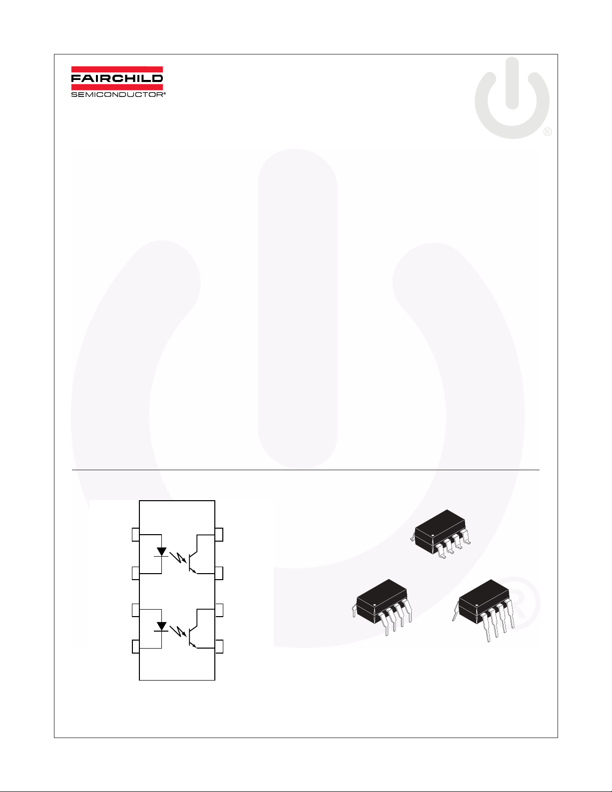
Schematic Package Outlines
ANODE
CATHODE
ANODE
CATHODE
1
2
3
4 5
Equivalent Circuit
©2003 Fairchild Semiconductor Corporation www.fairchildsemi.com
MCT9001 Rev. 1.0.7
COLLECTOR
8
EMITTER
7
COLLECTOR
6
EMITTER
8
1
8
1
8
1

MCT9001 — Dual Phototransistor Optocouplers
Absolute Maximum Ratings
Stresses exceeding the absolute maximum ratings may damage the device. The device may not function or be
operable above the recommended operating conditions and stressing the parts to these levels is not recommended.
In addition, extended exposure to stresses above the recommended operating conditions may affect device reliability.
The absolute maximum ratings are stress ratings only.
Symbol Rating Value Unit
TOTAL DEVICE
T
Storage Temperature -55 to +150 °C
STG
T
Operating Temperature -55 to +100 °C
OPR
T
SOL
P
Total Device Power Dissipation @ T
D
EMITTER (Each channel)
Forward Current – Continuous 60 mA
I
F
(pk) Forward Current – Peak (PW = 1µs, 300pps) 3 A
I
F
V
Reverse Voltage 5.0 V
R
P
LED Power Dissipation @ T
D
DETECTOR (Each channel)
Collector Current – Continuous 30 mA
I
C
P
D
Lead Solder Temperature
(Refer to Reflow Temperature Profile)
= 25°C 400 mW
A
260 for 10 sec °C
Derate above 25°C 4.83 mW/°C
= 25°C 100 mW
A
Derate above 25°C (Total Input) 1.1 mW/°C
Detector Power Dissipation @ T
= 25°C 150 mW
A
Derate above 25°C 1.67 mW/°C
©2003 Fairchild Semiconductor Corporation www.fairchildsemi.com
MCT9001 Rev. 1.0.7 2

≤
Ω
MCT9001 — Dual Phototransistor Optocouplers
Electrical Characteristics
(T
= 25°C unless otherwise specified)
A
Individual Component Characteristics
Symbol Parameter Test Conditions Min. Typ.* Max. Unit
EMITTER
V
I
C
Input Forward Voltage I
F
Reverse Current V
R
Junction Capacitance V
J
= 10mA 1.0 1.3 V
F
= 5V 10 µA
R
= 0 V, f = 1MHz 50 pF
F
DETECTOR
BV
BV
I
CEO
C
Collector-Emitter Breakdown Voltage I
CEO
Emitter-Collector Breakdown Voltage I
ECO
Collector-Emitter Dark Current V
Capacitance V
CE
= 0.5mA, I
C
= 100µA, I
E
= 24V, I
CE
V
= 24V, T
CE
= 0V, f = 1MHz 8 pF
CE
= 0 55 V
F
= 0 7 V
F
= 0 5 100 nA
F
= 85°C 50 µA
A
Transfer Characteristics
Symbol Parameter Test Conditions Min. Typ.* Max. Units
SWITCHING TIMES (AC)
Non-Saturated
t
t
Turn-on Time R
on
Turn-off Time 3 µs
off
Rise Time 2.4 µs
t
r
t
Fall Time 2.4 µs
f
Saturated
t
t
Turn-on Time I
on
Turn-off Time 25.0 µs
off
DC CHARACTERISTICS
CTR Current Transfer Ratio,
CTR
V
CE(sat)
Collector-Emitter
(sat)
Saturation Voltage I
= 100 Ω , I
L
= 16mA, R
F
I
= 5mA, V
F
I
= 8mA, V
F
= 8mA, I
F
= 2mA, V
C
= 1.9k Ω , V
L
= 5V 50 600 %
CE
= 0.4V 30 %
CE
= 2.4mA 0.40 V
C
= 10V 3 µs
CC
= 5V 2.4 µs
CE
Isolation Characteristics
Symbol Characteristic Test Conditions Min. Typ.* Max. Units
V
Input-Output Isolation Voltage I
ISO
R
Isolation Resistance V
ISO
C
Isolation Capacitance f = 1MHz 0.5 pF
ISO
*All typicals at T
©2003 Fairchild Semiconductor Corporation www.fairchildsemi.com
MCT9001 Rev. 1.0.7 3
= 25°C
A
10µA, t = 1min. 5000 Vac(rms)
I-O
= 500VDC 10
I-O
11
 Loading...