

MCT5201M, MCT5210M, MCT5211M — Low Input Current Phototransistor Optocouplers
September 2009
MCT5201M, MCT5210M, MCT5211M
Low Input Current Phototransistor Optocouplers
Features
■
High CTR
CTR guaranteed 0°C to 70°C
■
■
High common mode transient rejection 5kV/µs
Data rates up to 150kbits/s (NRZ)
■
■
Underwriters Laboratory (UL) recognized,
file #E90700, volume 2
IEC60747-5-2 approved (ordering option V)
■
comparable to Darlingtons
CE(SAT)
Applications
■
CMOS to CMOS/LSTTL logic isolation
■
LSTTL to CMOS/LSTTL logic isolation
RS-232 line receiver
■
■
Telephone ring detector
AC line voltage sensing
■
■
Switching power supply
Description
The MCT52XXM series consists of a high-efficiency
AlGaAs, infrared emitting diode, coupled with an NPN
phototransistor in a six pin dual-in-line package.
The MCT52XXM is well suited for CMOS to LSTT/TTL
interfaces, offering 250% CTR
input current. When an LED input current of 1.6mA is
supplied data rates to 20K bits/s are possible.
The MCT52XXM can easily interface LSTTL to LSTTL/
TTL, and with use of an external base to emitter resistor
data rates of 100K bits/s can be achieved.
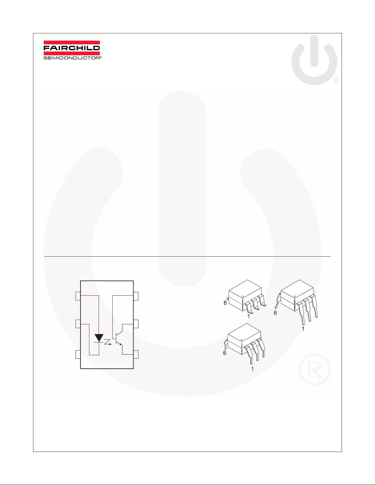
Schematic Package Outlines
with 1mA of LED
CE(SAT)
ANODE
CATHODE
©1983 Fairchild Semiconductor Corporation www.fairchildsemi.com
MCT5201M, MCT5210M, MCT5211M Rev. 1.1.3
1
2
3
6
BASE
5 COL
4 EMITTER

Absolute Maximum Ratings
Stresses exceeding the absolute maximum ratings may damage the device. The device may not function or be
operable above the recommended operating conditions and stressing the parts to these levels is not recommended.
In addition, extended exposure to stresses above the recommended operating conditions may affect device reliability.
The absolute maximum ratings are stress ratings only.
Symbol Parameters Value Units
TOTAL DEVICE
T
STG
T
OPR
T
SOL
P
EMITTER
I
V
(pk) Forward Current - Peak (1 µs pulse, 300 pps) 3.0 A
I
F
P
DETECTOR
I
P
Storage Temperature -55 to +150 °C
Operating Temperature -40 to +100 °C
Lead Solder Temperature 260 for 10 sec °C
Total Device Power Dissipation @ 25°C (LED plus detector) 260 mW
D
Derate Linearly From 25°C 3.5 mW/°C
Continuous Forward Current 50 mA
F
Reverse Input Voltage 6 V
R
LED Power Dissipation 75 mW
D
Derate Linearly From 25°C 1.0 mW/°C
Continuous Collector Current 150 mA
C
Detector Power Dissipation 150 mW
D
Derate Linearly from 25°C 2.0 mW/°C
MCT5201M, MCT5210M, MCT5211M — Low Input Current Phototransistor Optocouplers
©1983 Fairchild Semiconductor Corporation www.fairchildsemi.com
MCT5201M, MCT5210M, MCT5211M Rev. 1.1.3 2

∆
∆
Ω
MCT5201M, MCT5210M, MCT5211M — Low Input Current Phototransistor Optocouplers
Electrical Characteristics
(T
= 25°C unless otherwise specified)
A
Individual Component Characteristics
Symbol Parameters Test Conditions Device Min. Typ.* Max. Units
EMITTER
V
V
V
C
Input Forward Voltage I
F
Forward Voltage Temp. Coefficient I
F
T
A
Reverse Voltage I
R
Junction Capacitance V
J
= 5mA All 1.25 1.5 V
F
= 2mA All -1.75 mV/°C
F
= 10µA All 6 V
R
= 0V, f = 1.0MHz All 18 pF
F
DETECTOR
BV
BV
BV
I
CER
C
C
C
Collector-Emitter Breakdown Voltage I
CEO
Collector-Base Breakdown Voltage I
CBO
Emitter-Base Breakdown Voltage I
EBO
Collector-Emitter Dark Current V
Capacitance, Collector to Emitter V
CE
Capacitance, Collector to Base V
CB
Capacitance, Emitter to Base V
EB
= 1.0mA, I
C
= 10µA, I
C
= 10µA, I
E
= 10V, I
CE
R
= 1M Ω
BE
= 0, f = 1MHz All 10 pF
CE
= 0, f = 1MHz All 80 pF
CB
= 0, f = 1MHz All 15 pF
EB
= 0 All 30 100 V
F
= 0 All 30 120 V
F
= 0 All 5 10 V
F
= 0,
F
All 1 100 nA
Isolation Characteristics
Symbol Characteristic Test Conditions Device Min. Typ.* Max. Units
V
R
C
CM
CM
*All typical T
Input-Output Isolation
ISO
ISO
ISO
H
(10)
Voltage
Isolation Resistance
Isolation Capacitance
Common Mode Transient V
Rejection – Output HIGH V
Common Mode Transient V
L
Rejection – Output LOW V
= 25°C
A
(10)
f = 60Hz, t = 1 sec. All 7500 Vac(peak)
11
(9)
V
= 500 VDC, T
I-O
V
= 0, f = 1 MHz All 0.4 0.6 pF
I-O
= 50 V
CM
= 0
I
F
= 50 V
CM
= 0
I
F
= 50 V
CM
=1.6mA
I
F
= 50 V
CM
= 5mA
I
F
= 25°C All 10
A
P-P1
P-P
P-P1
P-P1
, R
, R
, R
, R
= 750 Ω ,
L
= 1K Ω ,
L
= 750 Ω ,
L
= 1K Ω ,
L
MCT5210M/11M 5000 V/µs
MCT5201M
MCT5210M/11M 5000 V/µs
MCT5201M
©1983 Fairchild Semiconductor Corporation www.fairchildsemi.com
MCT5201M, MCT5210M, MCT5211M Rev. 1.1.3 3

MCT5201M, MCT5210M, MCT5211M — Low Input Current Phototransistor Optocouplers
Electrical Characteristics
(Continued) (T
= 25°C unless otherwise specified)
A
Transfer Characteristics
Symbol Characteristics Test Conditions Device Min. Typ.* Max. Units
DC CHARACTERISTICS
CTR
CE(SAT)
Saturated Current
Tr ansfer Ratio
(Collector to Emitter)
CTR
Current Transfer Ratio
(CE)
(Collector to Emitter)
CTR
Current Transfer Ratio
(CB)
Collector to Base
V
CE(SAT)
Saturation Voltage IF = 5mA, ICE = 6mA MCT5201M 0.4 V
AC CHARACTERISTICS
T
PHL
Propagation Delay
HIGH-to-LOW
T
PLH
Propagation Delay
LOW-to-HIGH
d
t
r
s
t
f
Delay Time
Rise Time
Storage Time
Fall Time
= 25°C
A
t
t
*All typicals at T
(1)
(3)
(4)
(5)
(6)
(7)
(8)
I
(2)
= 5mA, V
F
= 3.0mA, V
I
F
= 1.6mA, V
I
F
= 1.0mA, V
I
F
I
= 3.0mA, V
F
(1)
= 1.6mA, V
I
F
= 1.0mA, V
I
F
I
= 5mA, VCB = 4.3V MCT5201M 0.28 %
F
= 3.0mA, VCE = 4.3V MCT5210M 0.2
I
F
= 1.6mA, VCE = 4.3V MCT5211M 0.3
I
F
= 1.0mA, VCE = 4.3V 0.25
I
F
= 3.0mA, ICE = 1.8mA MCT5210M 0.4
I
F
= 1.6mA, ICE = 1.6mA MCT5211M 0.4
I
F
= 0.4V MCT5201M 120 %
CE
= 0.4V MCT5210M 60
CE
= 0.4V MCT5211M 100
CE
= 0.4V 75
CE
= 5.0V MCT5210M 70 %
CE
= 5.0V MCT5211M 150
CE
= 5.0V 110
CE
RL = 330 Ω, RBE = ∞ IF = 3.0mA,
R
= 3.3 kΩ, R
L
= 750 Ω, RBE = ∞ IF = 1.6mA,
R
L
R
= 4.7 kΩ, RBE = 91kΩ 15
L
= 1.5 kΩ, RBE = ∞ IF = 1.0mA,
R
L
R
= 10 kΩ, RBE = 160kΩ 24
L
= 0.4V, VCC = 5V,
V
CE
= fig. 13, RBE = 330kΩ
R
L
= 39kΩ 7
BE
RL = 330 Ω, RBE = ∞ IF = 3.0mA,
R
= 3.3 kΩ, R
L
= 750 Ω, R
R
L
R
= 4.7 kΩ, R
L
= 1.5 kΩ, R
R
L
R
= 10 kΩ, R
L
= 0.4V, VCC = 5V,
V
CE
= fig. 13, RBE = 330kΩ
R
L
= 39kΩ 8
BE
= ∞ IF = 1.6mA,
BE
= 91kΩ 11
BE
= ∞ IF = 1.0mA,
BE
= 160kΩ 16
BE
VCE = 0.4V, RBE = 330kΩ,
= 1 kΩ, VCC = 5V
R
L
VCE = 0.4V, RBE = 330kΩ,
= 1 kΩ, VCC = 5V
R
L
VCE = 0.4V, RBE = 330 kΩ,
= 1 kΩ, VCC = 5V
R
L
VCE = 0.4V, RBE = 330 kΩ,
= 1 kΩ, VCC = 5V
R
L
MCT5210M 10 µs
= 5.0V
V
CC
MCT5211M 14
= 5.0V
V
CC
17
= 5.0V
V
CC
I
= 5mA MCT5201M 3 30
F
MCT5210M 0.4 µs
= 5.0V
V
CC
MCT5211M 2.5
= 5.0V
V
CC
7
= 5.0V
V
CC
I
= 5mA MCT5201M 12 13
F
I
= 5mA MCT5201M 1.1 15 µs
F
I
= 5mA MCT5201M 2.5 20 µs
F
I
= 5mA MCT5201M 10 13 µs
F
I
= 5mA MCT5201M 16 30 µs
F
©1983 Fairchild Semiconductor Corporation www.fairchildsemi.com
MCT5201M, MCT5210M, MCT5211M Rev. 1.1.3 4

Notes:
1. DC Current Transfer Ratio (CTR
current (I
) x 100%, at a specified voltage between the collector and emitter (VCE).
F
2. The collector base Current Transfer Ratio (CTR
divided by the input LED current (I
3. Referring to Figure 14 the T
) is defined as the transistor collector current (ICE) divided by the input LED
CE
) is defined as the transistor collector base photocurrent(ICB)
) time 100%.
F
propagation delay is measured from the 50% point of the rising edge of the data
PHL
CB
input pulse to the 1.3V point on the falling edge of the output pulse.
4. Referring to Figure 14 the T
propagation delay is measured from the 50% point of the falling edge of data input
PLH
pulse to the 1.3V point on the rising edge of the output pulse.
5. Delay time (t
6. Rise time (t
7. Storage time (t
8. Fall time (t
9. C
is the capacitance between the input (pins 1, 2, 3 connected) and the output, (pin 4, 5, 6 connected).
ISO
) is measured from 50% of rising edge of LED current to 90% of Vo falling edge.
d
) is measured from 90% to 10% of Vo falling edge.
r
) is measured from 50% of falling edge of LED current to 10% of Vo rising edge.
s
) is measured from 10% to 90% of Vo rising edge.
f
10. Device considered a two terminal device: Pins 1, 2, and 3 shorted together, and pins 5, 6 and 7 are shorted
together.
MCT5201M, MCT5210M, MCT5211M — Low Input Current Phototransistor Optocouplers
©1983 Fairchild Semiconductor Corporation www.fairchildsemi.com
MCT5201M, MCT5210M, MCT5211M Rev. 1.1.3 5

Safety and Insulation Ratings
As per IEC 60747-5-2, this optocoupler is suitable for “safe electrical insulation” only within the safety limit data.
Compliance with the safety ratings shall be ensured by means of protective circuits.
Symbol Parameter Min. Typ. Max. Unit
MCT5201M, MCT5210M, MCT5211M — Low Input Current Phototransistor Optocouplers
Installation Classifications per DIN VDE 0110/1.89
Ta ble 1
For Rated Main Voltage < 150Vrms I-IV
For Rated Main voltage < 300Vrms I-IV
Climatic Classification 55/100/21
Pollution Degree (DIN VDE 0110/1.89) 2
CTI Comparative Tracking Index 175
V
PR
Input to Output Test Voltage, Method b,
V
x 1.875 = VPR, 100% Production Test
IORM
1594 V
peak
with tm = 1 sec, Partial Discharge < 5pC
Input to Output Test Voltage, Method a,
V
x 1.5 = VPR, Type and Sample Test
IORM
1275 V
peak
with tm = 60 sec, Partial Discharge < 5pC
V
IORM
V
IOTM
Max. Working Insulation Voltage 850 V
Highest Allowable Over Voltage 6000 V
peak
peak
External Creepage 7 mm
External Clearance 7 mm
Insulation Thickness 0.5 mm
RIO Insulation Resistance at Ts, V
= 500V 10
IO
9
Ω
©1983 Fairchild Semiconductor Corporation www.fairchildsemi.com
MCT5201M, MCT5210M, MCT5211M Rev. 1.1.3 6

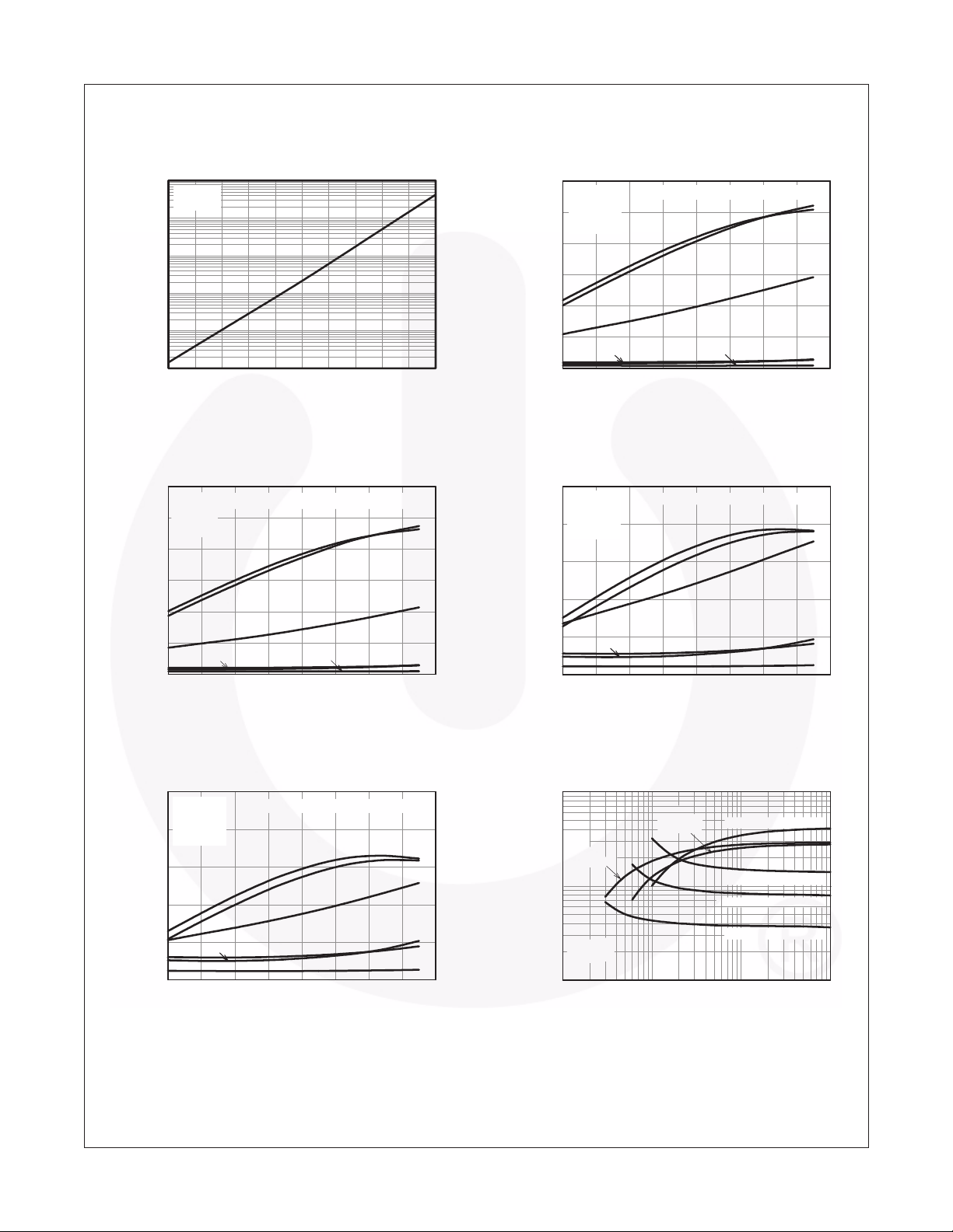
Typical Performance Curves
MCT5201M, MCT5210M, MCT5211M — Low Input Current Phototransistor Optocouplers
Fig. 1 LED Forward Voltage vs. Forward Current
2.0
1.8
1.6
1.4
TA = -40°C
1.2
TA = 25°C
– FORWARD VOLTAGE (V)
1.0
F
V
0.8
0.1 1 10
TA = 100°C
IF – LED FORWARD CURRENT (mA)
Fig. 3 Normalized CTR vs. Temperature
1.4
Normalized to:
= 5mA
I
F
1.2
1.0
0.8
0.6
0.4
0.2
0.0
NORMALIZED CURRENT TRANSFER RATIO
= 5V
V
CE
= 25°C
T
A
-40 -20 100 120
= 10mA
I
F
-20 0 20 40 60
– AMBIENT TEMPERATURE (°C)
T
A
= 5mA
I
F
I
= 2mA
F
= 1mA
I
F
= 0.5mA
I
F
I
= 0.2mA
F
1.4
1.2
1.0
0.8
0.6
0.4
0.2
0.0
100 0.1
NORMALIZED CURRENT TRANSFER RATIO
10
1
–
CE
0.1
0.01
NORMALIZED I
0.001
COLLECTOR-EMITTER CURRENT
0.0001
0.1 1 10
Fig. 2 Normalized Current Transfer Ratio vs.
Forward Current
Normalized to:
= 5mA
I
F
= 5V
V
CE
= 25°C
T
A
110
I
– FORWARD CURRENT (mA)
F
Fig. 4 Normalized Collector vs.
Collector-Emitter Voltage
I
= 10mA
F
I
= 5mA
I
F
= 1mA
I
F
= 0.5mA
I
F
IF = 0.2mA
Normalized to:
= 5mA
I
F
= 5V
V
CE
= 25°C
T
A
V
– COLLECTOR-EMITTER VOLTAGE (V)
CE
F
= 2mA
Fig. 5 Normalized Collector Base Photocurrent
Ratio vs. Forward Current
100
10
1
– COLLECTOR-BASE
CB
0.1
PHOTO CURRENT
0.01
NORMALIZED I
0.1 1 10010
– FORWARD CURRENT (mA)
I
F
Normalized to:
= 5mA
I
F
= 4.3V
V
CB
= 25°C
T
A
NORMALIZED COLLECTOR-BASE
Fig. 6 Normalized Collector-Base Current
vs. Temperature
10
= 10mA
I
F
I
= 5mA
1
0.1
CURRENT
0.01
Normalized to:
= 5mA
I
F
= 4.3V
V
CB
= 25°C
T
A
0.001
-60 -40 -20 0 20 40 60 80 100
– AMBIENT TEMPERATURE (°C)
T
A
F
= 1mA
I
F
I
= 0.5mA
F
IF = 0.2mA
= 2mA
I
F
©1983 Fairchild Semiconductor Corporation www.fairchildsemi.com
MCT5201M, MCT5210M, MCT5211M Rev. 1.1.3 7
Typical Performance Curves (Continued)
MCT5201M, MCT5210M, MCT5211M — Low Input Current Phototransistor Optocouplers
Fig. 7 Collector-Emitter Dark Current vs.
Ambient Temperature
10000
IF = 0mA
= 10V
V
CE
1000
100
10
– DARK CURRENT (nA)
1
CEO
I
0.1
0102030405060708090
TA – AMBIENT TEMPERATURE (°C) TA – AMBIENT TEMPERATURE (°C)
Fig. 9 Switching Time vs.
30
I
= 10mA
F
V
CC
25
= 1kΩ
R
L
R
BE
20
15
10
t – SWITCHING TIME (µs)
5
0
Ambient Temperature
Refer to Figure 13 for switching time circuit
= 5V
= 100kΩ
t
f
t
PLH
t
s
t
r
– AMBIENT TEMPERATURE (°C)
T
A
t
PHL
t
d
100
120-40 -20 0 20 40 60 80 100
Fig. 8 Switching Time vs.
30
IF = 10mA
V
CC
25
= 1kΩ
R
L
R
BE
20
15
10
t – SWITCHING TIME (µs)
5
0
Ambient Temperature
= 5V
= 330kΩ
Refer to Figure 13 for switching time circuit
t
f
t
r
t
t
PHL
PLH
t
s
t
d
120-40 -20 0 20 40 60 80 100
Fig. 10 Switching Time vs.
Ambient Temperature
20
= 5mA
I
F
= 5V
V
CC
= 1kΩ
R
L
16
= 330kΩ
R
BE
12
8
4
t – SWITCHING TIME (µs)
0
Refer to Figure 13 for switching time circuit
t
f
t
PLH
t
s
t
r
t
PHL
t
d
TA – AMBIENT TEMPERATURE (°C)
120-20-40 0 20 40 60 80 100
Fig. 11 Switching Time vs.
20
= 5mA
I
F
V
CC
R
L
16
R
BE
12
8
4
t – SWITCHING TIME (µs)
0
-40 -20 0 20 40 60 80 100 120
Ambient Temperature
= 5V
= 1kΩ
= 100kΩ
Refer to Figure 13 for switching time circuit
t
f
t
PLH
t
s
t
r
– AMBIENT TEMPERATURE (°C) RBE – BASE-EMITTER RESISTANCE (kΩ)
T
A
t
PHL
t
d
100
t
PLH
IF = 3mA
RL = 3.3kΩ
10
VCC = 5V
t – SWITCHING TIME (µs)
T
1
10 100 1000 10000
Fig. 12 Switching Time vs.
Base-Emitter Resistance
t
PLH
IF = 1.6mA
RL = 4.7kΩ
= 25°C
A
t
, IF = 1mA, RL = 10kΩ
PLH
t
, IF = 1mA, RL = 10kΩ
PHL
t
, IF = 1.6mA, RL = 4.7kΩ
PHL
t
, IF = 3mA, RL = 3.3kΩ
PHL
©1983 Fairchild Semiconductor Corporation www.fairchildsemi.com
MCT5201M, MCT5210M, MCT5211M Rev. 1.1.3 8

MCT5201M, MCT5210M, MCT5211M — Low Input Current Phototransistor Optocouplers
Typical Electro-Optical Characteristics (T
V
= 5.0 V
CC
Pulse Gen
= 50Ω
Z
O
f = 10KHz
10% D.F.
monitor
I
F
100 Ω
tr, tf, td, t
s
TEST CIRCUIT
0
330K
INPUT
(I
1K
V
O
Figure 13.
50%
)
F
t
d
= 25°C unless otherwise specified)
A
= 5.0 V
V
CC
Pulse Gen
= 50Ω
Z
O
f = 10KHz
10% D.F.
monitor
I
F
100 Ω
330K
t
TEST CIRCUIT
1K 4.7K
D1
V
O
, t
PHL
PLH
D2
D3
D4
OUTPUT
)
(V
O
0
90%
t
PHL
t
1.3 V
PLH
1.3 V
10% 10%
t
r
t
s
Figure 14. Switching Circuit Waveforms
90%
t
f
©1983 Fairchild Semiconductor Corporation www.fairchildsemi.com
MCT5201M, MCT5210M, MCT5211M Rev. 1.1.3 9

Package Dimensions
Through Hole 0.4" Lead Spacing
8.13–8.89
64
8.13–8.89
64
MCT5201M, MCT5210M, MCT5211M — Low Input Current Phototransistor Optocouplers
6.10–6.60
5.08 (Max.)
3.28–3.53
0.38 (Min.)
(0.86)
1.02–1.78
Pin 1
13
0.41–0.51
0.25–0.36
0.76–1.14
2.54–3.81
2.54 (Bsc)
Surface Mount
7.62 (Typ.)
15° (Typ.)
8.13–8.89
64
0.20–0.30
6.10–6.60
5.08 (Max.)
3.28–3.53
0.38 (Min.)
(0.86)
1.02–1.78
Pin 1
13
0.41–0.51
(1.78)
0.25–0.36
0.76–1.14
2.54–3.81
2.54 (Bsc)
(1.52)
0.20–0.30
10.16–10.80
(2.54)
(0.76)
8.43–9.90
6.10–6.60
Pin 1
(7.49)
(10.54)
13
Rcommended Pad Layout
0.25–0.36
3.28–3.53
5.08
(Max.)
0.38 (Min.)
(0.86)
1.02–1.78
0.41–0.51
0.76–1.14
2.54 (Bsc)
0.16–0.88
(8.13)
0.20–0.30
Note:
All dimensions in mm.
©1983 Fairchild Semiconductor Corporation www.fairchildsemi.com
MCT5201M, MCT5210M, MCT5211M Rev. 1.1.3 10

Ordering Information
Order Entry Identifier
Option
No suffix MCT5201M Standard Through Hole Device (50 units per tube)
S MCT5201SM Surface Mount Lead Bend
SR2 MCT5201SR2M Surface Mount; Tape and Reel (1,000 units per reel)
T MCT5201TM 0.4" Lead Spacing
V MCT5201VM IEC60747-5-2
TV MCT5201TVM IEC60747-5-2, 0.4" Lead Spacing
SV MCT5201SVM IEC60747-5-2, Surface Mount
SR2V MCT5201SR2VM IEC60747-5-2, Surface Mount, Tape and Reel (1,000 units per reel)
(Example) Description
Marking Information
1
MCT5201M, MCT5210M, MCT5211M — Low Input Current Phototransistor Optocouplers
MCT5201
V X YY Q
43
5
2
6
Definitions
1Fairchild logo
2Device number
VDE mark (Note: Only appears on parts ordered with VDE
3
option – See order entry table)
4 One digit year code, e.g., ‘7’
5Two digit work week ranging from ‘01’ to ‘53’
6 Assembly package code
*Note – Parts that do not have the ‘V’ option (see definition 3 above) that are marked with
date code ‘325’ or earlier are marked in portrait format.
©1983 Fairchild Semiconductor Corporation www.fairchildsemi.com
MCT5201M, MCT5210M, MCT5211M Rev. 1.1.3 11

Carrier Tape Specification
4.5 ± 0.20
0.30 ± 0.05
21.0 ± 0.1
0.1 MAX
User Direction of Feed
Reflow Profile
4.0 ± 0.1
10.1 ± 0.20
12.0 ± 0.1
2.0 ± 0.05
1.5 MIN
Ø
11.5 ± 1.0
9.1 ± 0.20
1.5 ± 0.1/-0
Ø
MCT5201M, MCT5210M, MCT5211M — Low Input Current Phototransistor Optocouplers
1.75 ± 0.10
24.0 ± 0.3
°C
300
280
260°C
260
240
220
200
180
160
Time above
183°C = 90 Sec
140
120
100
1.822°C/Sec Ramp up rate
80
60
40
20
33 Sec
0
0 60 180120 270
Time (s)
>245°C = 42 Sec
360
©1983 Fairchild Semiconductor Corporation www.fairchildsemi.com
MCT5201M, MCT5210M, MCT5211M Rev. 1.1.3 12

TRADEMARKS
The following includes registered and unregistered trademarks and service marks, owned by Fairchild Semiconductor and/or its global subsidiaries,andis not
intended to be an exhaustive list of all such trademarks.
Auto-SPM™
Build it Now™
CorePLUS™
CorePOWER™
CROSSVOLT™
CTL™
Current Transfer Logic™
EcoSPARK
EfficentMax™
EZSWITCH™*
®
™*
®
®
Fairchild
Fairchild Semiconductor
FACT Quiet Series™
®
FACT
®
FAST
®
F-PFS™
®
FRFET
Global Power Resource
Green FPS™
Green FPS™ e-Series™
Gmax™
GTO™
IntelliMAX™
ISOPLANAR™
MegaBuck™
MICROCOUPLER™
MicroFET™
MicroPak™
MillerDrive™
MotionMax™
Motion-SPM™
OPTOLOGIC
OPTOPLANAR
®
FastvCore™
FETBench™
FlashWriter
FPS™
®
*
PDP SPM™
Power-SPM™
PowerTrench
SM
PowerXS™
Programmable Active Droop™
QFET
QS™
Quiet Series™
RapidConfigure™
Saving our world, 1mW/W/kW at a time™
SmartMax™
SMART START™
SPM
STEALTH™
SuperFET™
®
®
SuperSOT™-3
SuperSOT™-6
SuperSOT™-8
SupreMOS™
SyncFET™
Sync-Lock™
®
®
ThePower Franchise
TinyBoost™
TinyBuck™
®
TinyLogic
®
TINYOPTO™
™
TinyPower™
TinyPWM™
TinyWire™
TriFault Detect™
®
TRUECURRENT™*
µSerDes™
®
UHC
Ultra FRFET™
UniFET™
VCX™
VisualMax™
®
*
XS™
*Trademarks of System General Corporation, used under license by Fairchild Semiconductor.
DISCLAIMER
FAIRCHILD SEMICONDUCTOR RESERVES THE RIGHT TO MAKE CHANGES WITHOUT FURTHER NOTICE TO ANY PRODUCTS HEREIN TO IMPROVE
RELIABILITY, FUNCTION, OR DESIGN. FAIRCHILD DOES NOT ASSUME ANY LIABILITY ARISING OUT OF THE APPLICATION OR USE OF ANY PRODUCT OR
CIRCUIT DESCRIBED HEREIN; NEITHER DOES IT CONVEY ANY LICENSE UNDER ITS PATENT RIGHTS, NOR THE RIGHTS OF OTHERS. THESE
SPECIFICATIONS DO NOT EXPAND THE TERMS OF FAIRCHILD’S WORLDWIDE TERMS AND CONDITIONS, SPECIFICALLY THE WARRANTY THEREIN,
WHICH COVERS THESE PRODUCTS.
MCT5201M, MCT5210M, MCT5211M — Low Input Current Phototransistor Optocouplers
LIFE SUPPORT POLICY
FAIRCHILD’S PRODUCTS ARE NOT AUTHORIZED FOR USE AS CRITICAL COMPONENTS IN LIFE SUPPORT DEVICES OR SYSTEMS WITHOUT THE
EXPRESS WRITTEN APPROVAL OF FAIRCHILD SEMICONDUCTOR CORPORATION.
As used herein:
1. Life support devices or systems are devices or systems which, (a) are
intended for surgical implant into the body or (b) support or sustain life,
and (c) whose failure to perform when properly used in accordance
with instructions for use provided in the labeling, can be reasonably
expected to result in a significant injury of the user.
2. A critical component in any component of a life support, device, or
system whose failure to perform can be reasonably expected to
cause the failure of the life support device or system, or to affect its
safety or effectiveness.
ANTI-COUNTERFEITING POLICY
Fairchild Semiconductor Corporation's Anti-Counterfeiting Policy. Fairchild's Anti-Counterfeiting Policy is also stated on our external website, www.fairchildsemi.com,
under Sales Support.
Counterfeiting of semiconductor parts is a growing problem in the industry. All manufacturers of semiconductor products are experiencing counterfeiting of their parts.
Customers who inadvertently purchase counterfeit parts experience many problems such as loss of brand reputation, substandard performance, failedapplications,
and increased cost of production and manufacturing delays. Fairchild is taking strong measures to protect ourselves and our customers from the proliferation of
counterfeit parts. Fairchild strongly encourages customers to purchase Fairchild parts either directly from Fairchild or from Authorized Fairchild Distributors who are
listed by country on our web page cited above. Products customers buy either from Fairchild directly or from Authorized Fairchild Distributors are genuine parts, have
full traceability, meet Fairchild's quality standards for handling and storage and provide access to Fairchild's full range of up-to-date technicalandproduct information.
Fairchild and our Authorized Distributors will stand behind all warranties and will appropriately address any warranty issues that may arise. Fairchild will not provide
any warranty coverage or other assistance for parts bought from Unauthorized Sources. Fairchild is committed to combat this global problem and encourage our
customers to do their part in stopping this practice by buying direct or from authorized distributors.
PRODUCT STATUS DEFINITIONS
Definition of Terms
Datasheet Identification Product Status Definition
Advance Information Formative / In Design
Preliminary
First Production
No Identification Needed Full Production
Obsolete Not In Production
Datasheet contains the design specifications for product development. Specifications may change in
any manner without notice.
Datasheet contains preliminary data; supplementary data will be published at a later date. Fairchild
Semiconductor reserves the right to make changes at any time without notice to improve design.
Datasheet contains final specifications. Fairchild Semiconductor reserves the right to make changes
at any time without notice to improve the design.
Datasheet contains specifications on a product that is discontinued by Fairchild Semiconductor.
The datasheet is for reference information only.
Rev. I40
©1983 Fairchild Semiconductor Corporation www.fairchildsemi.com
MCT5201M, MCT5210M, MCT5211M Rev. 1.1.3 13
 Loading...