tm
HCPL062N 3.3V Dual Channel High Speed-10 MBit/s Logic Gate Optocouplers
July 2006
HCPL062N
3.3V Dual Channel High Speed-10 MBit/s Logic Gate
Optocouplers
Features
■
Compact SO8 package
Very high speed – 10MBit/s
■
■
Superior CMR – 25kV/µs minimum (1,000 volts
common mode)
Logic gate output
■
■
Wired OR-open collector
Fixed threshold detector design minimizes thermal
■
impact on switching times
■
U.L. recognized (File # E90700)
Applications
Ground loop elimination
■
■
Field buses
Line receiver, data transmission
■
■
Data multiplexing
■
Switching power supplies
Pulse transformer replacement
■
■
Computer-peripheral interface
Instrumentation input/output isolation
■
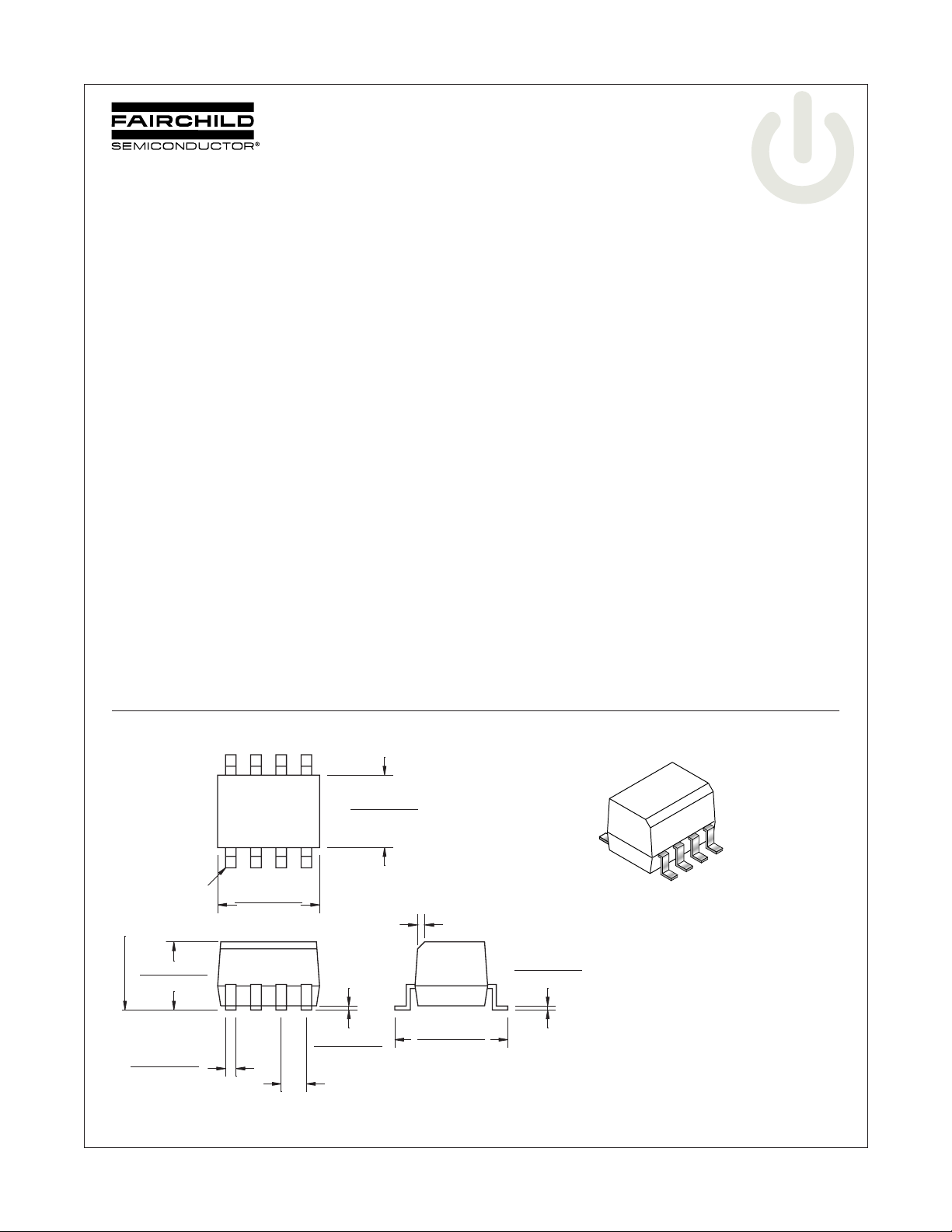
Package Dimensions
Description
The HCPL062N optocouplers consist of an AlGaAs LED,
optically coupled to a very high speed integrated photodetector logic gate consisting of bipolar transistors on a
CMOS process for reduced power consumption. The
output features an open collector, thereby permitting
wired OR outputs. The devices are housed in a compact
small-outline package. The coupled parameters are
guaranteed over the temperature range of -40°C to
+85°C. An internal noise shield and provides superior
common mode rejection.
NG PLANE
SEATI
Pin 1
0.143 (3.63)
0.123 (3.13)
0.021 (0.53)
0.011 (0.28)
0.202 (5.13)
0.182 (4.63)
Note:
All dimensions are in inches (millimeters)
©2006 Fairchild Semiconductor Corporation
HCPL062N Rev. 1.0.0
0.164 (4.16)
0.144 (3.66)
0.008 (0.20)
0.003 (0.08)
0.050 (1.27)
TYP
0.019 (0.48)
0.244 (6.19)
0.224 (5.69)
1
0.010 (0.25)
0.006 (0.16)
Lead Coplanarity : 0.004 (0.10) MAX
www.fairchildsemi.com

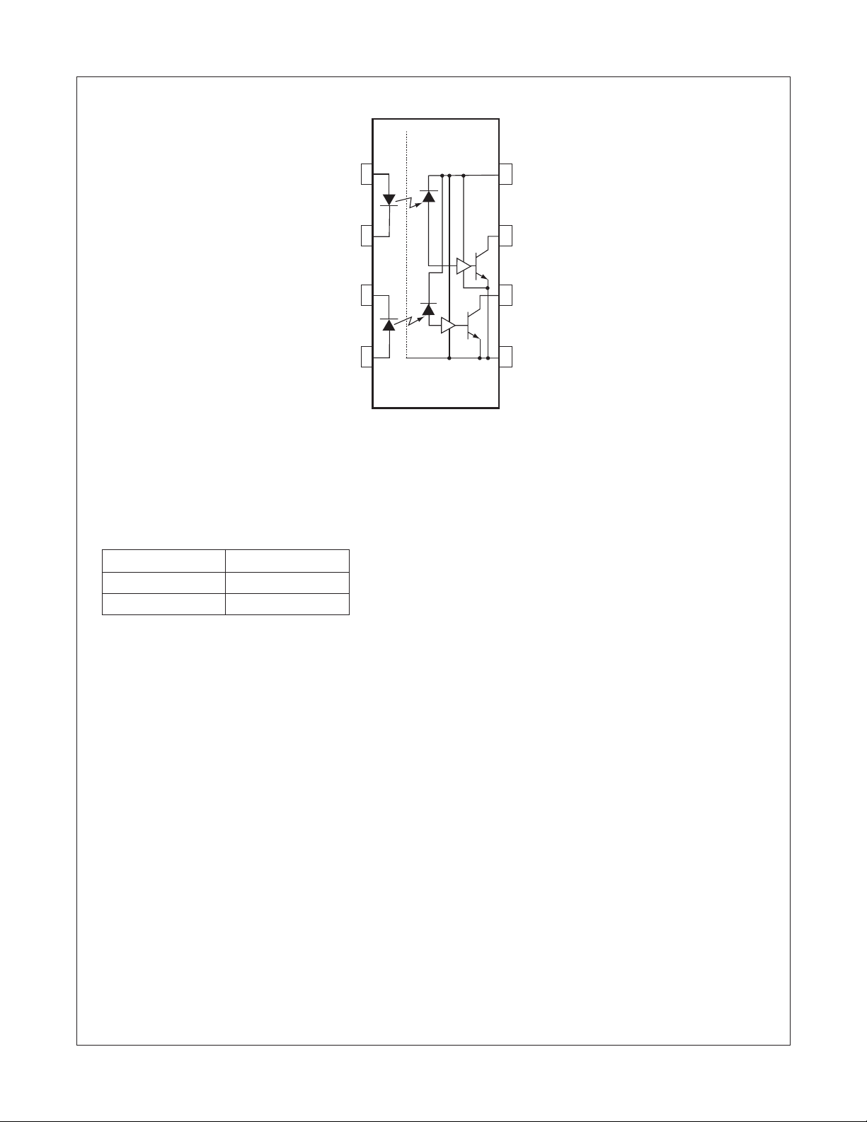
Circuit Drawing
HCPL062N 3.3V Dual Channel High Speed-10 MBit/s Logic Gate Optocouplers
(1)
+
1
V
F1
_
2
_
3
V
F2
+
4 5
8
7
6
V
CC
V
01
V
02
GND
Note:
1. The V
or solid tantalum capacitor with good high frequency characteristic and should be connected no further than 3mm
from the V
supply to each optoisolator must be bypassed by a 0.1µF capacitor or larger. This can be either a ceramic
CC
and GND pins of each device.
CC
Truth Table (Positive Logic)
Input Output
HL
LH
A 0.1µF bypass capacitor must be connected between pins 8 and 5.
HCPL062N Rev. 1.0.0
2
www.fairchildsemi.com

HCPL062N 3.3V Dual Channel High Speed-10 MBit/s Logic Gate Optocouplers
Absolute Maximum Ratings
(No derating required up to 85°C)
Symbol Parameter Value Units
T
STG
T
OPR
EMITTER
I
F
V
R
P
I
DETECTOR
V
CC
(1 minute max)
I
O
V
O
P
O
Storage Temperature -40 to +125 °C
Operating Temperature -40 to +85 °C
DC/Average Forward Input Current (each channel) 50 mA
Reverse Input Voltage (each channel) 5.0 V
Power Dissipation 45 mW
Supply Voltage 7.0 V
Output Current (each channel) 15 mA
Output Voltage (each channel) 7.0 V
Collector Output Power Dissipation 85 mW
Recommended Operating Conditions
Symbol Parameter Min. Max. Units
I
FL
I
FH
V
CC
T
A
NFan Out (TTL load) – 5 TTL Loads
R
L
Note:
2. 6.3mA is a guard banded value which allows for at least 20% CTR degradation. Initial input current threshold value
is 5.0mA or less
Input Current, Low Level 0 250 µA
Input Current, High Level 6.3
(2)
15 mA
Supply Voltage, Output 2.7 3.3 V
Operating Temperature -40 +85 °C
Output Pull-up 330 4K
Ω
HCPL062N Rev. 1.0.0
3
www.fairchildsemi.com

∆
/ ∆
HCPL062N 3.3V Dual Channel High Speed-10 MBit/s Logic Gate Optocouplers
Electrical Characteristics
(T
= -40°C to +85°C Unless otherwise specified.)
A
Individual Component Characteristics
Symbol Parameter Test Conditions Min. Typ.
EMITTER
V
B
Input Forward Voltage I
F
Input Reverse Breakdown
VR
= 10mA – – 1.8 V
F
T
=25°C – – 1.75
A
I
= 10µA 5.0 – – V
R
Voltage
V
T
F
Input Diode Temperature
A
I
= 10mA – -1.5 – mV/°C
F
Coefficient
DETECTOR
I
CCH
I
CCL
Switching Characteristics
High Level Supply Current I
Low Level Supply Current I
(T
= -40°C to +85°C, V
A
= 0mA, V
F
= 10mA, V
F
CC
= 3.3V – 7.1 10 mA
CC
= 3.3V – 6.7 15 mA
CC
= 3.3V, I
= 7.5 mA Unless otherwise specified.)
F
Symbol AC Characteristics Test Conditions Min. Typ.
T
PLH
Propagation Delay
Time to Output High
Level
T
PHL
Propagation Delay
Time to Output Low
Level
|T
–T
PHL
| Pulse Width Distortion R
PLH
t
Output Rise Time
r
(10–90%)
t
Output Fall Time
f
(90–10%)
| Common Mode
|CM
H
Tr ansient Immunity
(at Output High Level)
| Common Mode
|CM
L
Tr ansient Immunity
(at Output Low Level)
R
= 350 Ω , C
L
= 15pF
L
Note 4, Fig. 10
= 350 Ω , C
R
L
= 15pF
L
Note 5, Fig. 10
= 350 Ω , C
L
= 15pF
L
Fig. 10
R
= 350 Ω , C
L
= 15pF)
L
Note 6, Fig. 10
R
= 350 Ω , C
L
= 15pF
L
Note 7, Fig. 10
R
= 350 Ω , T
L
= 3.3V, V
V
CC
|V
| = 1,000V
CM
= 25°C, I
A
O(Min.)
Notes 8, 11, Fig. 11
R
= 350 Ω , T
L
= 3.3V, V
V
CC
|V
| = 1,000V
CM
=25°C, I
A
O(Max.)
Notes 9, 11, Fig. 11
F
= 2V
= 7.5mA,
F
= 0.8V
= 0 mA,
––90ns
––75ns
––25ns
–16–ns
–4–ns
25,000 – – V/µs
25,000 – – V/µs
(3)
Max. Unit
(3)
Max. Unit
HCPL062N Rev. 1.0.0
4
www.fairchildsemi.com
 Loading...