HC-MOS Power Dissipation
HC-CMOS Power Dissipation AN-303
Fairchild Semiconductor
Application Note 303
February 1984
If there is one single characteristic that justifies the existence
of CMOS, it is low power dissipation. In the quiescent state,
high-speed CMOS draws five to seven orders of magnitude
less power than the equivalent LSTTL function. When
switching, the amount of power dissipated by both metal
gate and high-speed silicon gate CMOS is directly proportional to the operating frequency of the device. This is because the higher the operating frequency, the more often the
device is being switched. Since each transition requires
power, power consumption increases with frequency.
First, one will find a description of the causes of power consumption in HC-CMOS and LSTTLapplications.Nextwillfollow a comparison of MM54HC/MM74HC to LSTTL power
dissipation. Finally, the maximum ratings for power dissipation imposed by the device package will be discussed.
Quiescent Power Consumption
Ideally, when a CMOS integrated circuit is not switching,
there should be no DC current paths from V
and the device should not draw any supply current at all.
to ground,
CC
However, due to the inherent nature of semiconductors, a
small amount of leakage current flows across all
reverse-biased diode junctions on the integrated circuit.
These leakages are caused by thermally-generated charge
carriers in the diode area.Asthetemperatureofthe diode increases, so do the number of these unwanted charge carriers, hence leakage current increases.
Leakage current is specified for all CMOS devices as I
This is the DC current that flows from V
inputs are held at either V
open. This is known as the quiescent state.
or ground, and all outputs are
CC
For the MM54HC/MM74HC family, I
ent temperatures (T
three different specifications at each temperature, depend-
) of 25˚C, 85˚C, and 125˚C. There are
A
to ground when all
CC
is specified at ambi-
CC
CC
ing on the complexity of the device. The number of diode
junctions grows with circuit complexity, thereby increasing
the leakage current. The worst case I
MM54HC/MM74HC family are summarized in
dition, it should be noted that the maximum I
decrease as the temperature goes below 25˚C.
TABLE 1. Supply Current (I
Specified at V
T
A
Gate Buffer MSI Unit
specifications for the
CC
Table1
current will
CC
) for MM54HC/MM74HC
CC
=
6V
CC
.Inad-
25˚C 2.0 4.0 8.0 µA
85˚C 20 40 80 µA
125˚C 40 80 160 µA
To obtain the quiescent power consumption for any CMOS
device, simply multiply I
=
DC
I
CCVCC
by the supply voltage: P
CC
Sample calculations show that at room temperature the
maximum power dissipation of gate, buffer, and MSI circuits
=
at V
6V are 10 µW, 20 µW, and 40 µW, respectively.
CC
Dynamic Power Consumption
Dynamic power consumption is basically the result of charging and discharging capacitances. It can be broken down
into three fundamental components, which are:
1. Load capacitance transient dissipation
2. Internal capacitance transient dissipation
3. Current spiking during switching.
Load Capacitance Transient Dissipation
The first contributor to power consumption is the charging
and discharging of external load capacitances.
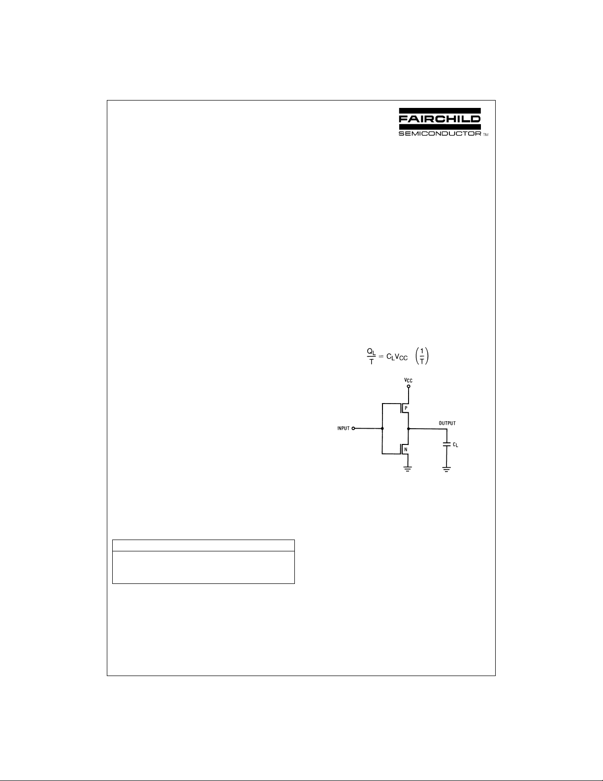
Figure 1
schematic diagram of a simple CMOS inverter driving a capacitive load. A simple expression for power dissipation as a
function of load capacitance can be derived starting with:
=
Q
C
L
LVCC
where CLis the load capacitance, and QLis the charge on
the capacitor. If both sides of the equation are divided by the
time required to charge and discharge the capacitor (one period, T, of the input signal), we obtain:
.
AN005021-1
FIGURE 1. Simple CMOS Inverter Driving a
Capacitive External Load
Since charge per unit time is current (QL/T=l) and the inverse of the period of a waveform is frequency (1/T=f):
=
l
f
C
L
LVCC
To find the power dissipation, both sides of the equation
must be multiplied by the supply voltage (P=Vl), yielding:
=
P
L
C
LVCC
2f
One note of caution is in order. If all the outputs of a device
are not switching at the same frequency,then the power consumption must be calculated at the proper frequency for
each output:
=
P
2(CL1f1+CL2f2+...+CLnfn)
V
L
CC
Examples of devices for which this may apply are: counters,
dual flip-flops with independent clocks, and other integrated
circuits containing dual, triple, etc., independent circuits.
is a
© 1998 Fairchild Semiconductor Corporation AN005021 www.fairchildsemi.com

Internal Capacitance Transient Dissipation
Internal capacitance transient dissipation is similar to load
capacitance dissipation, except that the internal parasitic
“on-chip” capacitance is being charged and discharged.
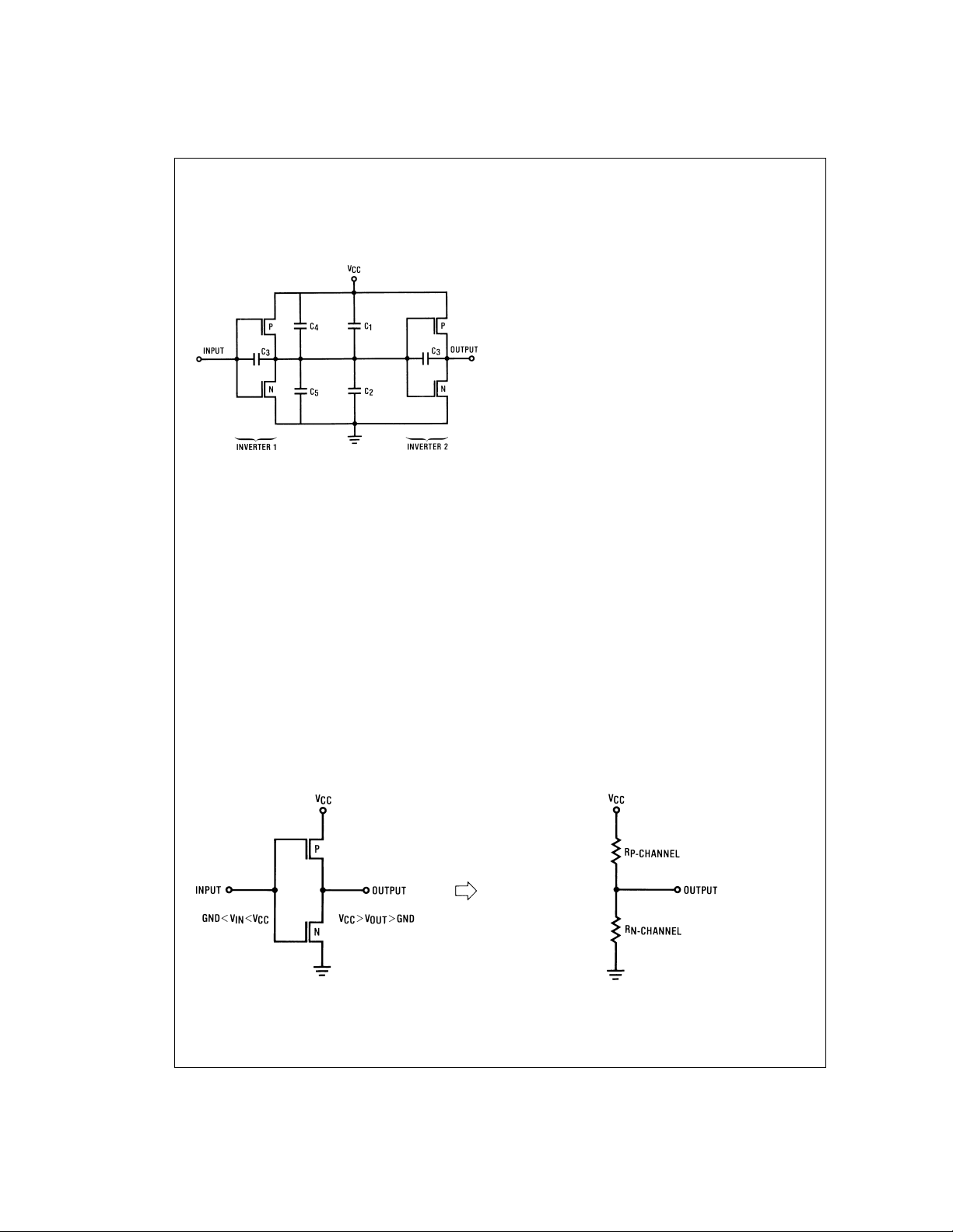
ure 2
is a diagram of the parasitic nodal capacitances asso-
Fig-
ciated with two CMOS inverters.
AN005021-2
FIGURE 2. Parasitic Internal Capacitances
Associated with Two Inverters
and C2are capacitances associated with the overlap of
C
1
the gate area and the source and channel regions of the Pand N-channel transistors, respectively. C
overlap of the gate and source (output), and is known as the
Miller capacitance. C
sitic diodes from the output to V
Thus the total internal capacitance seen by inverter 1 driving
and C5are capacitances of the para-
4
and ground, respectively.
CC
is due to the
3
inverter 2 is:
=
C
l
C
1+C2
+2C3+C4+C
5
Since an internal capacitance may be treated identically to
an external load capacitor for power consumption calculations, the same equation may be used:
=
P
2f
C
l
lVCC
At this point, it may be assumed that different parts of the internal circuitry are operating at different frequencies. Although this is true, each part of the circuit has a fixed frequency relationship between it and the rest of the device.
Thus, one value of an effective C
the internal power dissipation at any frequency. More will be
can be used to compute
l
said about this shortly.
Current Spiking During Switching
The final contributor to power consumption is current spiking
during switching. While the input to a gate is making a transition between logic levels, both the P- and N-channel transistors are turned partially on. This creates a low impedance
path for supply current to flow from V
trated in
Figure 3
.
to ground, as illus-
CC
For fast input rise and fall times (shorter than 50 ns for the
MM54HC/MM74HC family), the resulting power consumption is frequency dependent. This is due to the fact that the
more often a device is switched, the more often the input is
situated between logic levels, causing both transistors to be
partially turned on. Since this power consumption is proportional to input frequency and specific to a given device in any
application, as is C
ing term is called “C
pacitance. It is specified for every MM54HC/MM74HC de-
, it can be combined with Cl. The result-
l
” the no-load power dissipation ca-
PD,
vice in the AC Electrical Characteristic section of each data
sheet.
It should be noted that as input rise and fall times become
longer, the switching current power dissipation becomes
more dependent on the amount of time that both the P- and
N-channel transistors are turned on, and less related to C
as specified in the data sheets.
of the effective value of C
crease for the MM54HC/MM74HC08, MM54HC/
Figure 4
as input rise and fall times in-
PD
is a representation
MM74HC139, and MM54HC/MM74HC390. To get a fair
comparison between the three curves, each is divided by the
value of C
fall times. This is represented by “C
specified in the data sheets for each part. This comparison
appears in
for the particular device with fast input rise and
PD
Figure 5
.CPDremains constant for input rise and
” the value of C
PD0,
fall times up to about 20 ns, after which it rises, approaching
a linear slope of 1. The graphs do not all reach a slope of 1
at the same time because of necessary differences in circuit
design for each part. The MM54HC/MM74HC08 exhibits the
greatest change in C
shows less of an increase in C
Thus, the power dissipation for most of the parts in the
, while the MM54HC/MM74HC139
PD
at any given frequency.
PD
MM54HC/MM74HC family will fall within these two curves.
One notable exception is the MM54HC/MM74HCU04.
PD
PD
AN005021-3
FIGURE 3. Equivalent schematic of a CMOS inverter whose input is between logic levels
www.fairchildsemi.com 2
AN005021-4
 Loading...