H11AG1M — Phototransistor Optocoupler
September 2009
H11AG1M
Phototransistor Optocoupler
Features
■
High efficiency low degradation liquid epitaxial IRED
Logic level compatible, input and output currents,
■
with CMOS and LS/TTL
■
High DC current transfer ratio at low input currents
(as low as 200µA)
■
Underwriters Laboratory (UL) recognized File
#E90700, Volume 2
IEC 60747-5-2 approved (ordering option V)
■
Applications
■
CMOS driven solid state reliability
■
Telephone ring detector
Digital logic isolation
■
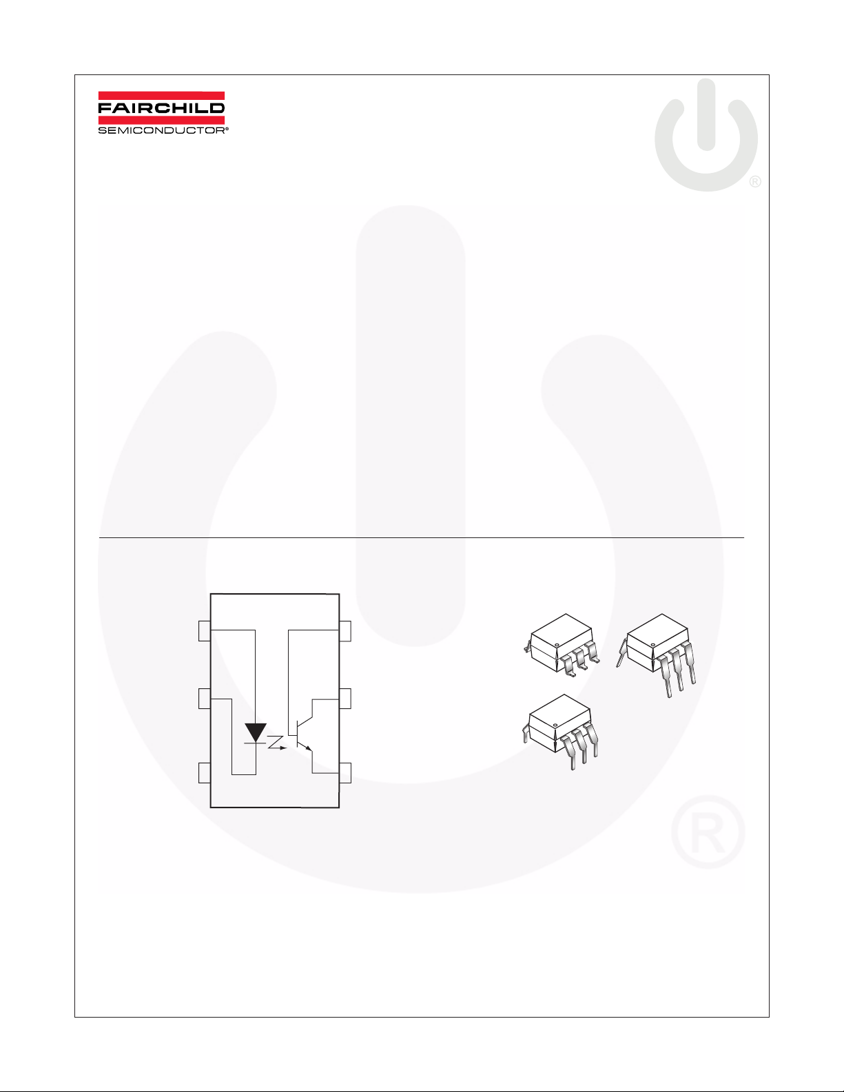
Schematic
ANODE
1
6
BASE
Description
The H11AG1M device consists of a Gallium-AluminumArsenide IRED emitting diode coupled with a silicon
phototransistor in a dual in-line package. This device
provides the unique feature of the high current transfer
ratio at both low output voltage and low input current.
This makes it ideal for use in low power logic circuits,
telecommunications equipment and portable electronics
isolation applications.
6
1
N/C
2
3
5 COL
4 EMITTER
6
1
CATHODE
©2007 Fairchild Semiconductor Corporation www.fairchildsemi.com
H11AG1M Rev. 1.0.3
6
1

Absolute Maximum Ratings
Stresses exceeding the absolute maximum ratings may damage the device. The device may not function or be
operable above the recommended operating conditions and stressing the parts to these levels is not recommended.
In addition, extended exposure to stresses above the recommended operating conditions may affect device reliability.
The absolute maximum ratings are stress ratings only.
Symbol Parameters Value Units
TOTAL DEVICE
T
STG
T
OPR
T
SOL
P
D
EMITTER
I
F
V
R
I
(pk) Forward Current – Peak (1µs pulse, 300pps) 3.0 A
F
P
D
DETECTOR
P
D
I
C
Storage Temperature -55 to +150 °C
Operating Temperature -40 to +100 °C
Lead Solder Temperature (Wave Solder) 260 for 10 sec °C
Total Device Power Dissipation @ 25°C (LED plus detector)
Derate Linearly From 25°C
260 mW
3.5 mW/°C
Continuous Forward Current 50 mA
Reverse Voltage 6 V
LED Power Dissipation 25°C Ambient
Derate Linearly From 25°C
Detector Power Dissipation @ 25°C
Derate Linearly from 25°C
75 mW
1.0 mW/°C
150 mW
2.0 mW/°C
Continuous Collector Current 50 mA
H11AG1M — Phototransistor Optocoupler
©2007 Fairchild Semiconductor Corporation www.fairchildsemi.com
H11AG1M Rev. 1.0.3 2

(T
Electrical Characteristics
= 25°C unless otherwise specified.)
A
Individual Component Characteristics
Symbol Parameters Test Conditions Min. Typ.* Max. Units
EMITTER
V
I
C
DETECTOR
BV
BV
BV
I
CEO
C
*Typical values at T
Input Forward Voltage I
F
Reverse Leakage Current V
R
Capacitance V = 0, f = 1.0MHz 100 pF
J
Breakdown Voltage, Collector to Emitter I
CEO
Collector to Base I
CBO
Emitter to Collector I
ECO
Leakage Current, Collector to Emitter V
Capacitance V
CE
= 25°C.
A
= 1mA 1.25 1.5 V
F
= 5V, T
R
= 1.0mA, I
C
= 100µA, I
C
= 100µA, I
C
CE
CE
= 25°C 10 µA
A
= 0 30 V
F
= 0 70 V
F
= 0 7 V
F
= 10V, I
= 0 5 10 µA
F
= 10V, f = 1MHz 10 pF
H11AG1M — Phototransistor Optocoupler
Isolation Characteristics
Symbol Parameter Test Conditions Min. Typ.* Max. Units
V
ISO
R
ISO
Input-Output Isolation Voltage f = 60Hz, t = 1 sec. 7500
Isolation Resistance V
Transfer Characteristics
= 500VDC, T
I-O
(T
= 25°C Unless otherwise specified.)
A
= 25°C 10
A
11
V
AC
Symbol Characteristics Test Conditions Min. Typ.* Max. Units
DC CHARACTERISTICS
CTR Current Transfer Ratio I
V
CE(SAT)
Saturation Voltage I
AC CHARACTERISTICS
Non-Saturated Switching Times
t
on
t
off
*Typical values at T
Tu r n-On Time R
Tu r n-Off Time R
= 25°C
A
= 1mA, V
F
I
= 1mA, V
F
I
= 0.2mA, V
F
= 2.0mA, I
F
= 100 Ω , I
L
= 100 Ω , I
L
= 5V 300 %
CE
= 0.6V 100
CE
= 1.5V 100
CE
= 0.5mA .40 V
C
= 1mA, V
F
= 1mA, V
F
= 5V 5 µs
CC
= 5V 5 µs
CC
PEAK
Ω
©2007 Fairchild Semiconductor Corporation www.fairchildsemi.com
H11AG1M Rev. 1.0.3 3
 Loading...