

Fairchild GreenBridge FDMQ8203, GreenBridge FDMS86200, GreenBridge FDMS8025S, GreenBridge FDMC2523P User Manual
Page 1

Is Now Part of
To learn more about ON Semiconductor, please visit our website at
ON Semi conductor an d the ON Semico nductor logo a re trademar ks of Semicon ductor Comp onents Indus tries, L LC dba ON Semico nductor or it s subsidiari es in the United S tates and /or other coun tries. ON Se miconducto r owns the righ ts to a number
of patents, trademarks, copyrights, trade secrets, and other intellectual property. A listing of ON Semiconductor’s product/patent coverage may be accessed at www.onsemi.com/site/pdf/Patent-Marking.pdf. ON Semiconductor reserve s the right
to make changes without f urther noti ce to any produc ts herein. ON S emicon ductor makes no warran ty, representat ion or guar antee regar ding the suitability of its pro ducts for any partic ular purpose, n or does ON Semic onductor as sume any liabilit y
arisin g out of the applica tion or us e of any product o r circui t, and specific ally dis claims any and all lia bilit y, includin g witho ut limit ation sp ecial, c onsequential or incidental da mages . Buye r is responsib le for it s products and a pplica tions us ing ON
Semic onductor pr oducts, inc luding complia nce with all law s, regulati ons and safet y requirem ents or stan dards, rega rdless of an y support or ap plications in formation p rovided by ON S emiconduc tor. “Typical ” parameter s which may be pr ovided in ON
Semic onductor data s heet s and/or s pecificatio ns can and do vary in diff erent a pplica tions an d actual perf ormance may var y over time. All o perat ing parameter s, including “Typical s” must b e validated for e ach cus tomer ap plicat ion by customer’s
techni cal exper ts. ON Semic onductor do es not conve y any license un der its pate nt rights no r the rights o f others. ON S emiconduc tor produc ts are not des igned, inte nded, or autho rized for use a s a critical c omponent in lif e support s ystems or an y FDA
Clas s 3 medical devi ces or medica l devices wit h a same or similar c lassificat ion in a foreign j urisdictio n or any device s intended for im plantation in t he human body. Sho uld Buyer pur chase or use ON S emiconduct or products f or any such unint ended
or unaut horized appli cation, Buy er shall indemn ify and hold O N Semiconduc tor and its of ficers, e mployees , subsidiari es, affilia tes, and dis tributor s harmless ag ainst all claim s, costs , damages, an d expenses , and reason able attorn ey fees aris ing out
of, dire ctly or indire ctly, any claim o f personal inj ury or death as sociated w ith such unint ended or unauth orized use, e ven if such claim a lleges that ON S emiconduc tor was neglig ent regardin g the design or ma nufacture o f the part. ON S emiconduct or
is an Equa l Oppor tunity/Affirm ative Action E mployer. This li terature is s ubject to all applicable c opyright la ws and is no t for resale in any manner.
www.onsemi.com
Page 2

User Guide for
GreenBridge™ Evaluation Kit
for Power Over Ethernet 90 W Active
Clamp Forward DC-DC Converter
MLP 4.5x5 GreenBridge™
Power 33/56 Shielded Gate PowerTrench® MOSFET
Featured Fairchild Products:
FDMQ8203
FDMS86200
FDMS8025S
FDMC2523P
Direct questions or comments
about this evaluation board to:
“Worldwide Direct Support”
Fairchild Semiconductor.com
© 2013 Fairchild Semiconductor Corporation FEBFDMQ8203_90W • Rev. 1.0.1
Page 3

Table of Contents
1. Introduction ............................................................................................................................... 3
1.1. Description ......................................................................................................................3
2. General Evaluation Board Specifications ................................................................................. 4
3. Photographs............................................................................................................................... 5
4. Setup and Test Procedure .......................................................................................................... 6
4.1. Hardware Connector Description ....................................................................................6
5. Performance of Evaluation Board ............................................................................................. 7
6. Printed Circuit Board .............................................................................................................. 10
7. Schematic ................................................................................................................................ 11
8. Bill of Materials ...................................................................................................................... 13
9. Revision History ..................................................................................................................... 15
© 2013 Fairchild Semiconductor Corporation 2 FEBFDMQ8203_90W • Rev. 1.0.1
Page 4
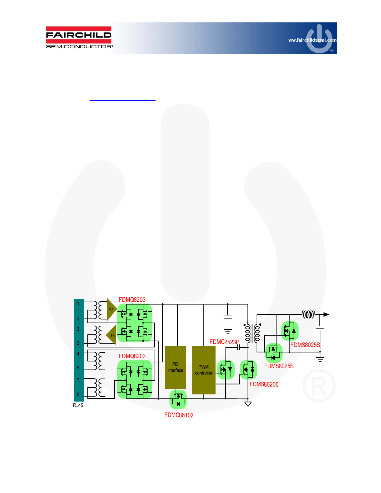
This user guide supports the evaluation kit for GreenBridge™ and shielded gate
PowerTrench
(PoE). It should be used in conjunction with their datasheets as well as Fairchild’s
application notes and technical support team. Please visit Fairchild’s website at
www.fairchildsemi.com
1. Introduction
This document describes the proposed solution for PoE++ PD that increases the
delivering power up to 90 W. It is designed to rectify a polarity of DC voltage from
Power Source Equipment (PSE) and then active clamp forward DC-DC converter steps
down a nominal input voltage 48 V
switching frequency. To deliver 90 W power through a network cable, the power system
is composed with four-pair architecture, which PSE uses to deliver data and power to the
PD through both the spare pair and data pair in the network cable at the same time.
1.1. Description
GreenBridge™ FDMQ8203 replaces the conventional diode bridge to reduce the power
dissipation caused by the large voltage drop of a diode bridge, resulting in a lower power
class power device. The small package size of MLP4.5x5 reduces PCB area and increases
power density. FDMC86102 100 V shielded gate PowerTrench® MOSFET for the hot
swap switch has the low conduction loss and the ruggedness due to the low R
wide safe operating area (SOA). The FDMS86200 150 V shielded gate PowerTrench
MOSFET reduces switching loss and conduction loss in the primary switch of the active
clamp forward topology because it has low FOM (R
shielded gate PowerTrench MOSFET is optimized for synchronous rectification because
it has the low R
®
MOSFET applying to a Power Device (PD) of Power over Ethernet
.
to output voltage 3.3 V
IN
and outstanding body diode performance.
DS(on)
x Qg). The FDMS8025S 30 V
DS(on)
in 300 kHz of the
OUT
DS(on)
and
Figure 1. Power diagram
© 2013 Fairchild Semiconductor Corporation 3 FEBFDMQ8203_90W • Rev. 1.0.1
Page 5
Table 1. MOSFET Parameters
Part Number Package Type BV
DSS
R
(V)
[mΩ]
DS(ON)
at 10 V
GS
Qg [nC]
at 10 VGS
C
[pF]
OSS
Max. Max. Max.
FDMQ8203 MLP 4.5x5
FDMC86102 POWER33 N-Ch 100 24 13 175
FDMS86200 POWER56 N-Ch 150 18 33 203
FDMC2523P POWER33 P-Ch -150 1500 9 80
FDMS8025S POWER56 N-Ch 30 2.8 34 815
N-Ch 100 110 5 55
P-Ch -80 190 19 65
2. General Evaluation Board Specifications
Table 2. Summary of Features and Performance
Description Value Remark
Input Voltage Range 42 ~ 57 VIN IEEE802.3 at Standard
Output Voltage Range 3.3 V
Switching Frequency 300 kHz Adjustable by R29 and R30, R31
Maximum Output Current 27 A Limited by Power Component
PCB Size 100x70 mm FR-4 / 4 Layers
PD Controller IEEE802.3 at PD Controller
PWM Controller Active Clamp Forward Controller
42V
>89%
IN
Efficiency
Temperature
48VIN >90%
57VIN >90%
FDMQ8203 58.4°C
FDMC86102 56.4°C
FDMS86200 74°C
FDMC2523P 65°C
FDMS8025S 88.6°C
Adjustable by R22 and R46
OUT
At Full Load (90 W)
At Full Load (25℃ Room Temperature)
© 2013 Fairchild Semiconductor Corporation 4 FEBFDMQ8203_90W • Rev. 1.0.1
Page 6
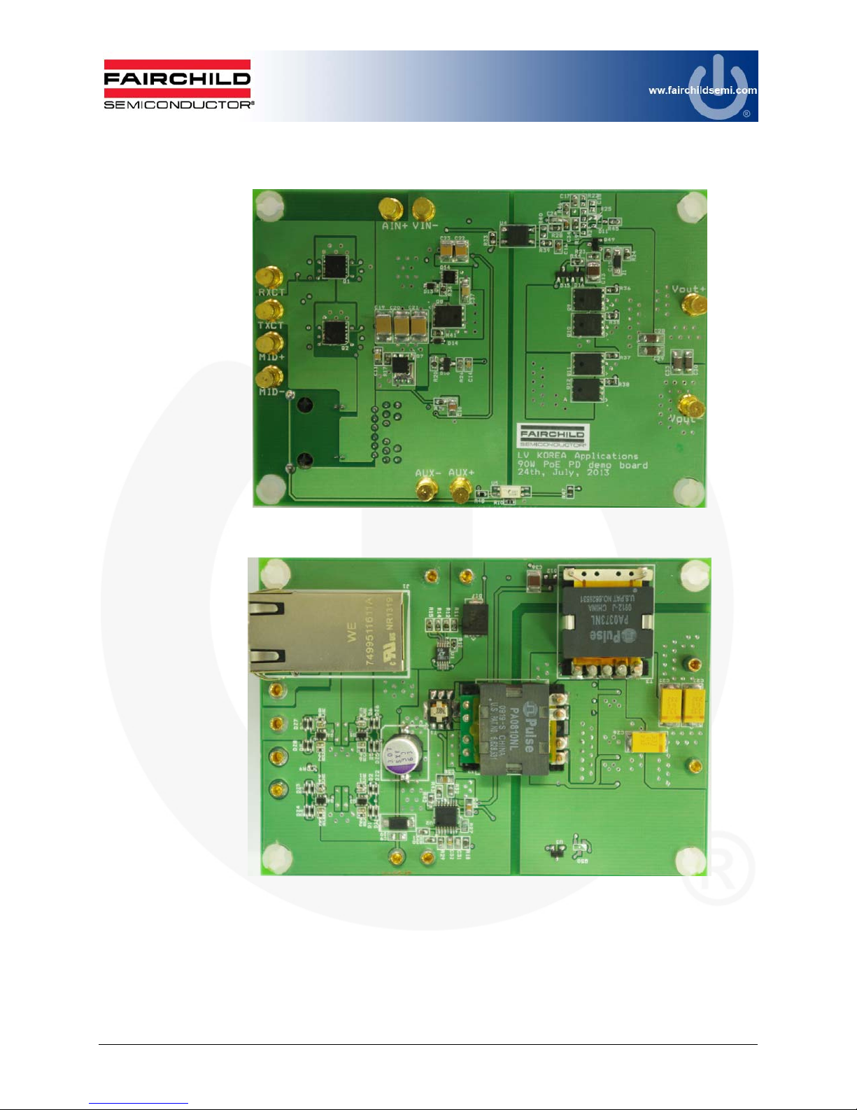
3. Photographs
Figure 2. Top Side View of Evaluation Kit
Figure 3. Bottom Side View of Evaluation Kit
© 2013 Fairchild Semiconductor Corporation 5 FEBFDMQ8203_90W • Rev. 1.0.1
Page 7

4. Setup and Test Procedure
Table 3. Test Point Descriptions
Test Point Label Descriptions
J6 AUX+ Measurement test point for positive AUX input voltage
J7 AUX- Measurement test point for negative AUX input voltage
J8 VIN+ Measurement test point for rectified positive input voltage
J9 VIN- Measurement test point for input voltage return
J10 +VOUT Measurement test point for output voltage
J11 -VOUT Measurement test point for output voltage return
4.1. Hardware Connector Description
The evaluation kit is fully assembled and tested. Follow the steps below to verify board
operation.
1. Use one of the following methods to power the evaluation kit:
If network connectivity is required:
Connect a network cable from the evaluation kit input port RJ45 connector to the
corresponding PSE Ethernet LAN connection, which provides power to the
evaluation kit such as PoE++ or four-fair architecture.
If network connectivity is not required:
Connect a -48 V DC power supply between the TXCT and RXCT; and
Connect a -48 V DC power supply between the MID+ and MID- together.
Caution: Do not turn on the power supply until all connections are completed.
2. Activate the PSE power supply or turn on the external DC power supply.
3. Using a voltmeter, verify that the evaluation kit provides +3.3 V across the
+VOUT and –VOUT pins. –VOUT is isolated from the evaluation kit’s input
VIN- and AUX- pins.
Figure 4. Test Setup
© 2013 Fairchild Semiconductor Corporation 6 FEBFDMQ8203_90W • Rev. 1.0.1
Page 8

5. Performance of Evaluation Board
Figure 5 through Figure 9 show the measured efficiency and power loss on the evaluation
board when operated under the conditions in Table 4. This board is optimized for
3.3 V
Table 4. Test Conditions
V
V
IN
42 ~ 57 V 3.3 V 300 kHz 0~27 A, 5 A Step, 3-minute soak time No
, 300 kHz fSW, and peak 27 A I
OUT
f
OUT
I
SW
specifications.
OUT
Cooling
OUT
Figure 5. Efficiency at V
Figure 6. Power Loss at V
=3.3 V, fSW=300 kHz, Soaking=3 Minutes, TA=25°C
OUT
=3.3 V, fSW=300 kHz, Soaking=3 Minutes, TA=25°C
OUT
© 2013 Fairchild Semiconductor Corporation 7 FEBFDMQ8203_90W • Rev. 1.0.1
Page 9

Figure 7. Thermal Performance Comparison: GreenBridge™ vs. Diode Bridge
=3.3, fSW= 300 kHz, Soaking=3 Minutes, TA=25°C
at V
OUT
GreenBridge™
FDMQ8203: 58.4°C
Forward Primary
FDMS86200: 74.0°C
Forward Secondary
FDMS8025S: 88.6°C
Figure 8. Top-Side Thermal Data at VIN=48 V, V
© 2013 Fairchild Semiconductor Corporation 8 FEBFDMQ8203_90W • Rev. 1.0.1
=3.3 / I
Soaking=10 Minutes, T
OUT
= 27 A, fSW= 300 kHz,
OUT
=25°C
A
Page 10

42 V
48 V
S210 Diode Bridge FDMQ8203 GreenBridge™
IN
89.6°C 63.0°C
IN
83.8°C 58.3°C
57 V
IN
77.0°C 55.2°C
Figure 9. Thermal Image Comparison: GreenBridge™ vs. Diode Bridge
V
OUT
=3.3 V, I
= 27 A, fSW=300 kHz, Soaking=3 Minutes, TA=25°C
OUT
© 2013 Fairchild Semiconductor Corporation 9 FEBFDMQ8203_90W • Rev. 1.0.1
Page 11

6. Printed Circuit Board
PCB layout (100 mm x 70 mm, 4-Layer, FR-4).
Figure 10. SST (Top Side) Layer
Figure 12. TOP & SMT Layer Figure 13. BOT & SMB Layer
Figure 11. SSB (Bottom Side) Layer
Figure 14. INNER1 (POWER) Layer Figure 15. INNER2 (GND) Layer
© 2013 Fairchild Semiconductor Corporation 10 FEBFDMQ8203_90W • Rev. 1.0.1
Page 12

7. Schematic
1
TRC T112TRD 1+
TRD 1-
10
4
BAS516
D4
D3
MM5Z10V
DZ4
DZ3
101112
9
12345
MM5Z10V
DZ2
BAS516
D2
BAS516
D7
MM5Z1 0V
DZ7
101112
12345
IN FROM PSE OUT TO PHY
11
5
6
Q4
BC846
R3
20K/1005
1nF/1005
C3
1234
8
Q1
FDMQ8203
67
C2
1nF/1005
123 4
R2
20K/1005
BC846
Q3
5
6
5
6
Q6
BC846
R7
20K/1005
1nF/1005
C7
1234
8
9
Q2
FDMQ8203
67
1000pF / 2KV
75Ohm X 4
7499511611A
R10
0
J2
TXCT
J3
RXCT
J4
MID +
J5
MID -
J12
SUPPORT
1
1
J13
SUPPORT
1
1
J14
SUPPORT
1
1
J15
SUPPORT
1
1
AUX-
J7
1
1
R12
20k
R14
49.9
R15
120
5
LT4275A
PWRGD
T2P
6
T2P
82k
R11
R13
0
IEEUVLO1AUX2RCLASS3RCLASS++4GND
U1
0.1uF/100 V
C10
HSGATE
HSSRC
VPORT
R16
8.2
8
9
7
10
56nF/100V
PWRGD
FDMC86102
Q7
R17
3.3K
C11
12nF X 4
4
523
7
J1
21
SHIELD
22
SHIELD
20
Green_C
19
Orange_C
18
Yellow_A
17
Yellow_C
1
1
1
1
1
1
1
1
P48V
P48V
8
TRD 4-
RXCT
TXCT
MID+
MID-
13
15
16
9
14
AUX+
J6
1
1
D17 S310
TRC T47TRD 4+
6
TRC T3
TRD 3+3TRD 2+
TRC T2
TRD 3-
TRD 2-
2
5
1
6
8
R4
20K/1005
BAS516
1nF/1005
C4
MM5Z10V
16
15
14
13
MM5Z10V
DZ1
C1
1nF/1005
BAS516
D1
R1
20K/1005
R8
20K/1005
BAS516
1nF/1005
C8
D8
MM5Z1 0V
DZ8
16
15
14
13
Figure 16. GreenBridge™ & PD controller Block Schematic
© 2013 Fairchild Semiconductor Corporation 11 FEBFDMQ8203_90W • Rev. 1.0.1
MM5Z1 0V
MM5Z1 0V
DZ5
DZ6
+
C12
33uF/63V
VIN+
C5
1nF/1005
R5
20K/1005
BAS516
BAS516
D6
D5
5
R9 20K/1005
D9 SMAJ58A
C9 NC
C6
1nF/1005
123 4
BC846
R6
20K/1005
Q5
6
P48V
P48V
Page 13

R31
8.2k
R30
56k
75k
R29
C32
0.1u
C31
100p
68k
R27
910
R18
CS
8
RTDEL1RTON2RTOFF3VREF4SYNC5GND6CS7RSLOPE
UCC2891D
SS/SD
FB
9
C35
0.22u/100V
R43
1k
PWRGD
4
SFH690BT
U4
1
23
R40
NC
23
U3
TLV431
1
82n
R28
12k
C34
330p
C24
U2
LINEUV
PGND
VDD
OUT
AUX
VIN
16
13
15
11
14
12
10
+
C22
47uF/16V
+
C23
47uF/16V
R42
27k
P_BIAS
R33
2k
R39
499
R22
820
NC
MMSZ5231B / 5.1Vz
Z1
1
2
C15 1uF
R24
10k
MMBT222 2A
0.1u
C16
R46
16k
C17
NC
Q50
NC
C18
NC
CS
C14
10n
2.2
R41
2.2
FDMS86200
Q8
10u/35V
C13
R23
499
Q49
R19
28k
51
R21
NC
R25
NC
D11
R26
12
D10
BAT54
1N4148WS
C38
0.22u/100V
R32
D13
R34
1K
4
D14
1N4148WS
R44
10
Q9
FDMS8025S
R45
G
1
S
2
S
3
S
Q54
FDMC2523P
PA0810NL
BAT54
D16
D15
BAT54
2.2
Q10
FDMS8025S
R36
FDMS8025S
Q11
FDMS8025S
Q12
1
VOUT-
J11
1
GND
1
1
R20 1k
3 7
5
D
6
D
7
D
8
D
9
D
12345
6
7810
2.2
R37
2.2
R38
2.2
+
C25
330uF / 6.3V
+
C26
330uF / 6.3V
+
C27
330uF / 6.3V
C28
22uF/6.3V
C29
22uF/6.3V
C33
22uF/6.3V
C30
22uF/6.3V
J9
VIN+
1
1
1
2.2uF/100V
C19
2.2uF/100V
C20
2.2uF/100V
C21
P8208
T1
8
C37 0.047uF /250V
T2
11
R35
11
7
1
VOUT+
1
Figure 17. Active Clamp Forward DC-DC Block Schematic
J8
VIN+
R48
50K 1%
T2P
U5
HMHA2801
PA0373NL
T3
1
6
D12
BAT54
10u/35V
C36
P_BIAS
20k
R47
J10
© 2013 Fairchild Semiconductor Corporation 12 FEBFDMQ8203_90W • Rev. 1.0.1
Page 14

8. Bill of Materials
# Qty. Reference Part Name Vendor Comment
1 8
2 8
3 1 C10 C2012X7R2A104K TDK
4 1 C11 VJ0805Y563KXBAT Vishay 56 nF 100 V / 2012
5 1 C12 63SXV33M Sanyo 33 µF / 63 V / Alu
6 2 C13,C36 CL32A106KLULNNE SAMSUNG 10µF / 35 V / 3225
7 1 C14 10 nF / 50 V Any 10 nF / 50 V / 1608
8 1 C15 1 µF / 50 V Any 1 µF / 50 V / 1608
9 2 C16,C32 0.1 µF / 50 V Any 0.1 µF / 50 V / 1608
10 3 C19,C20,C21 GRM32ER72A225KA35L MURATA
11 2 C22,C23 GRM32ER61C476ME15L MURATA 47 µF /16V/3225
12 1 C24 330 pF / 50 V Any 330 pF / 50 V / 1608
13 3 C25,C26,C27 T520D337M006ATE010 Kemet
14 4 C28,C29,C30,C33 C3216X5R0J226M TDK 22 µF /6.3V/3216
15 1 C31 100 pF / 50 V Any 100 pF / 50 V / 1608
16 1 C34 82 nF / 50 V Any 82 nF /50 V / 1608
17 2 C35,C38 C0805C224K1RACTU Kemet
18 1 C37 GRM31CR72E473KW03L MURATA 47 nF /250 V / 3210
19 8
20 8
21 1 D9 SMAJ58A Diodes TVS diode
22 4 D10,D12,D15,D16 BAT54 Fairchild Semiconductor BAT54
23 2 D13,D14 1N4148WS Fairchild Semiconductor 1N4148WS
24 1 D17 S310 Fairchild Semiconductor S310
25 1 J1 7499511611A Wurth Electronics
26 9
27 2 Q1,Q2 FDMQ8203 Fairchild Semiconductor
28 4 Q3,Q4,Q5,Q6 BC846BPDW1T1G ON Semiconductor
29 1 Q7 FDMC86102 Fairchild Semiconductor
30 1 Q8 FDMS86200 Fairchild Semiconductor
31 4 Q9,Q10,Q11,Q12 FDMS8025S Fairchild Semiconductor
C1,C2,C3,C4,C5,C6,C
7,C8
C9,D11,C17,C18,
R21,R25,R40,Q50
DZ1,DZ2,DZ3,DZ4,DZ
5,DZ6,DZ7,DZ8
D1,D2,D3,D4,D5,D6,D
7,D8
J2,J3,J4,J5,J6,J7,J8,J
9,J10,J11
1 nF / 1005 Any 1 nF / 50 V / 1005
NC
0.1 µF / 100 V /
2012
2.2 µF / 100 V /
3225
330 µF / 6.3 V /
Tantalum
220 nF /100 V /
2012
MM5Z10V Fairchild Semiconductor 10 V Zener Diode
BAS516 NXP Semiconductors
Test Pin Any 3 mm
SW 75 V 250 mA
HS
RJ45 w/
Transformer
GreenBridge™
Quad MOSFET
80 V Dual
Complementary
100 V 24 m
MOSFET
150 V 18 m
MOSFET
30 V 2.8 m
MOSFET
© 2013 Fairchild Semiconductor Corporation 13 FEBFDMQ8203_90W • Rev. 1.0.1
Page 15

# Qty. Reference Part Name Vendor Comment
32 1 Q49 MMBT2222A Fairchild Semiconductor NPN Transistor
33 1 Q54 FDMC2523P Fairchild Semiconductor
34 9
35 2 R10,R13 0 / 1608 Any 0 / 1608
36 1 R11 82 k / 1608 Any 82 k / 1608
37 2 R12,R47 20 k / 1608 Any 20 k / 1608
38 1 R14 49.9 / 1608 Any 49.9 / 1608
39 1 R15 120 / 1608 Any 120 / 1608
40 1 R16 8.2 / 1608 Any 8.2 / 1608
41 1 R17 3.3 k / 1608 Any 3.3 k / 1608
42 1 R18 910 / 1608 Any 910 / 1608
43 1 R19 28 k / 1608 Any 28 k / 1608
44 3 R20,R34,R43 1 k / 1608 Any 1 k / 1608
45 1 R22 820 / 1608 Any 820 / 1608
46 2 R23,R39 499 / 1608 Any 499 / 1608
47 1 R24 10 k / 1608 Any 10 k / 1608
48 1 R26 12 / 1608 Any 12 / 1608
49 1 R27 68 k / 1608 Any 68 k / 1608
50 1 R28 12 k / 1608 Any 12 k / 1608
51 1 R29 75 k / 1608 Any 75 k / 1608
52 1 R30 56 k / 1608 Any 56 k / 1608
53 1 R31 8.2 k / 1608 Any 8.2 k / 1608
54 6
55 1 R33 2 k / 1608 Any 2 k / 1608
56 1 R42 27 k / 1608 Any 27 k / 1608
57 1 R44 10 / 1608 Any 10 / 1608
58 1 R45 51 / 1608 Any 51 / 1608
59 1 R46 16 k / 1608 Any 16 k / 1608
60 1 R48 50 k Any 50 k
61 1 T1 P8208NL Pulse
62 1 T2 PA0810NL Pulse Inductor
63 1 T3 PA0373NL Pulse Transformer
64 1 U1 LT4275 Linear
65 1 U2 UCC2891PW Texas Instruments PWM Controller
66 1 U3 TLV431 Texas Instruments Shunt Regulator
67 1 U4 SFH690BT Vishay Semiconductors Phototransistor
68 1 U5 HMHA2801 Fairchild Semiconductor Opto-coupler
69 1 Z1 MMSZ5231B 5.1Vz Fairchild Semiconductor MMSZ5231B 5.1Vz
R1,R2,R3,R4,R5,R6,R
7,R8,R9
R32,R35,R36,R37,R38
,R41
20 k / 1005 Any 20 k / 1005
2.2 / 1608 Any 2.2 / 1608
(-)150 V 1.5
MOSFET
CURRENT SENSE
2000 µH
PoE++ PD
Controller
© 2013 Fairchild Semiconductor Corporation 14 FEBFDMQ8203_90W • Rev. 1.0.1
Page 16

9. Revision History
Rev. Date Description
1.0.0 September 2013 Initial Release
1.0.1 November 2013 Fixed typo table 4 VOUT to VIN
WARNING AND DISCLAIMER
Replace components on the Evaluation Board only with those parts shown on the parts list (or Bill of Materials) in the Users’ Guide. Contact an
authorized Fairchild representative with any questions.
This board is intended to be used by certified professionals, in a lab environment, following proper safety procedures. Use at your own risk. The
Evaluation board (or kit) is for demonstration purposes only and neither the Board nor this User’s Guide constitute a sales contract or create any kind
of warranty, whether express or implied, as to the applications or products involved. Fairchild warrantees that its products meet Fairchild’s published
specifications, but does not guarantee that its products work in any specific application. Fairchild reserves the right to make changes without notice to
any products described herein to improve reliability, function, or design. Either the applicable sales contract signed by Fairchild and Buyer or, if no
contract exists, Fairchild’s standard Terms and Conditions on the back of Fairchild invoices, govern the terms of sale of the products described herein.
DISCLAIMER
FAIRCHILD SEMICONDUCTOR RESERVES THE RIGHT TO MAKE CHANGES WITHOUT FURTHER NOTICE TO ANY PRODUCTS HEREIN TO
IMPROVE RELIABILITY, FUNCTION, OR DESIGN. FAIRCHILD DOES NOT ASSUME ANY LIABILITY ARISING OUT OF THE APPLICATION OR
USE OF ANY PRODUCT OR CIRCUIT DESCRIBED HEREIN; NEITHER DOES IT CONVEY ANY LICENSE UNDER ITS PATENT RIGHTS, NOR
THE RIGHTS OF OTHERS.
LIFE SUPPORT POLICY
FAIRCHILD’S PRODUCTS ARE NOT AUTHORIZED FOR USE AS CRITICAL COMPONENTS IN LIFE SUPPORT DEVICES OR SYSTEMS
WITHOUT THE EXPRESS WRITTEN APPROVAL OF THE PRESIDENT OF FAIRCHILD SEMICONDUCTOR CORPORATION.
As used herein:
1. Life support devices or systems are devices or systems which, (a)
are intended for surgical implant into the body, or (b) support or
sustain life, or (c) whose failure to perform when properly used in
accordance with instructions for use provided in the labeling, can be
reasonably expected to result in significant injury to the user.
ANTI-COUNTERFEITING POLICY
Fairchild Semiconductor Corporation's Anti-Counterfeiting Policy. Fairchild's Anti-Counterfeiting Policy is also stated on our external website,
www.fairchildsemi.com, under Sales Support.
Counterfeiting of semiconductor parts is a growing problem in the industry. All manufacturers of semiconductor products are experiencing
counterfeiting of their parts. Customers who inadvertently purchase counterfeit parts experience many problems such as loss of brand reputation,
substandard performance, failed applications, and increased cost of production and manufacturing delays. Fairchild is taking strong measures to
protect ourselves and our customers from the proliferation of counterfeit parts. Fairchild strongly encourages customers to purchase Fairchild parts
either directly from Fairchild or from Authorized Fairchild Distributors who are listed by country on our web page cited above. Products customers buy
either from Fairchild directly or from Authorized Fairchild Distributors are genuine parts, have full traceability, meet Fairchild's quality standards for
handling and storage and provide access to Fairchild's full range of up-to-date technical and product information. Fairchild and our Authorized
Distributors will stand behind all warranties and will appropriately address any warranty issues that may arise. Fairchild will not provide any warranty
coverage or other assistance for parts bought from Unauthorized Sources. Fairchild is committed to combat this global problem and encourage our
customers to do their part in stopping this practice by buying direct or from authorized distributors.
EXPORT COMPLIANCE STATEMENT
These commodities, technology, or software were exported from the United States in accordance with the Export Administration Regulations for the
ultimate destination listed on the commercial invoice. Diversion contrary to U.S. law is prohibited.
U.S. origin products and products made with U.S. origin technology are subject to U.S Re-export laws. In the event of re-export, the user will be
responsible to ensure the appropriate U.S. export regulations are followed.
2. A critical component is any component of a life support device or
system whose failure to perform can be reasonably expected to
cause the failure of the life support device or system, or to affect its
safety or effectiveness.
© 2013 Fairchild Semiconductor Corporation 15 FEBFDMQ8203_90W • Rev. 1.0.1
Page 17

ON Semiconductor and are trademarks of Semiconductor Components Industries, LLC dba ON Semiconductor or its subsidiaries in the United States and/or other countries.
ON Semiconductor owns the rights to a number of patents, trademarks, copyrights, trade secrets, and other intellectual property. A listing of ON Semiconductor’s product/patent
coverage may be accessed at www.onsemi.com/site/pdf/Patent−Marking.pdf
ON Semiconductor makes no warranty, representation or guarantee regarding the suitability of its products for any particular purpose, nor does ON Semiconductor assume any liability
arising out of the application or use of any product or circuit, and specifically disclaims any and all liability, including without limitation special, consequential or incidental damages.
Buyer is responsible for its products and applications using ON Semiconductor products, including compliance with all laws, regulations and safety requirements or standards,
regardless of any support or applications information provided by ON Semiconductor. “Typical” parameters which may be provided in ON Semiconductor data sheets and/or
specifications can and do vary in different applications and actual performance may vary over time. All operating parameters, including “Typicals” must be validated for each customer
application by customer’s technical experts. ON Semiconductor does not convey any license under its patent rights nor the rights of others. ON Semiconductor products are not
designed, intended, or authorized for use as a critical component in life support systems or any FDA Class 3 medical devices or medical devices with a same or similar classification
in a foreign jurisdiction or any devices intended for implantation in the human body. Should Buyer purchase or use ON Semiconductor products for any such unintended or unauthorized
application, Buyer shall indemnify and hold ON Semiconductor and its officers, employees, subsidiaries, affiliates, and distributors harmless against all claims, costs, damages, and
expenses, and reasonable attorney fees arising out of, directly or indirectly, any claim of personal injury or death associated with such unintended or unauthorized use, even if such
claim alleges that ON Semiconductor was negligent regarding the design or manufacture of the part. ON Semiconductor is an Equal Opportunity/Affirmative Action Employer. This
literature is subject to all applicable copyright laws and is not for resale in any manner.
PUBLICATION ORDERING INFORMATION
LITERATURE FULFILLMENT:
Literature Distribution Center for ON Semiconductor
19521 E. 32nd Pkwy, Aurora, Colorado 80011 USA
Phone: 303−675−2175 or 800−344−3860 Toll Free USA/Canada
Fax: 303−675−2176 or 800−344−3867 Toll Free USA/Canada
Email: orderlit@onsemi.com
© Semiconductor Components Industries, LLC
. ON Semiconductor reserves the right to make changes without further notice to any products herein.
N. American Technical Support: 800−282−9855 Toll Free
USA/Canada
Europe, Middle East and Africa Technical Support:
Phone: 421 33 790 2910
Japan Customer Focus Center
Phone: 81−3−5817−1050
ON Semiconductor Website: www.onsemi.com
Order Literature: http://www.onsemi.com/orderlit
For additional information, please contact your local
Sales Representative
www.onsemi.com
1
www.onsemi.com
 Loading...