Fairchild FSUSB22 service manual

March 2008
FSUSB22 — Low-Power, 2-Port, High-Speed USB 2.0
FSUSB22 — Low-Power, 2-Port, High-Speed USB 2.0 (480Mbps) Switch
(480Mbps) Switch
Features
-40dB Off Isolation at 250MHz
-40dB Non-adjacent Channel Crosstalk at 250MHz
On Resistance: 4.5Ω Typical (RON)
-3dB Bandwidth: 750MHz
Low-Power Consumption: 1µA Maximum
Control Input: TTL Compatible
Bi-directional Operation
USB High-Speed and Full-Speed Signaling
Capability
Applications
Cell Phones, PDAs, Digital Cameras, Notebook
Computers
Ordering Information
Operating
Part Number
FSUSB22BQX
FSUSB22QSC
FSUSB22QSCX
FSUSB22MTC
FSUSB22MTCX
All packages are lead free per JEDEC: J-STD-020B standard.
Temperature
Range
-40 to +85°C
-40 to +85°C
-40 to +85°C
-40 to +85°C
-40 to +85°C
16-Terminal Depopulated Quad Very-Thin Flat Pack No Leads
(DQFN), JEDEC MO-241, 2.5 x 3.5mm
16-Lead Quarter Size Outline Package (QSOP), JEDEC MO-137,
0.150-inch Wide
16-Lead Quarter Size Outline Package (QSOP), JEDEC MO-137,
0.150-inch Wide
16-Lead Thin Shrink Small Outline Package (TSSOP), JEDEC
MO-153, 4.4mm Wide
16-Lead Thin Shrink Small Outline Package (TSSOP), JEDEC
MO-153, 4.4mm Wide
Description
FSUSB22 is a low-power, high-bandwidth switch
specially designed for applications switching high-speed
USB 2.0 signals in handset and consumer applications;
such as cell phone, digital camera, and notebook with
hubs or controllers of limited USB I/O. The wide
bandwidth (750MHz) allows signals to pass with
minimum edge and phase distortion. Superior channelto-channel crosstalk results in minimal interference. It is
compatible with the USB2.0 Hi-Speed standard.
.
Package
Packing
Method
Tape and
Reel
Tube
Tape and
Reel
Tube
Tape and
Reel
©2005Fairchild Semiconductor Corporation www.fairchildsemi.com
FSUSB22 • Rev. 1.0.3

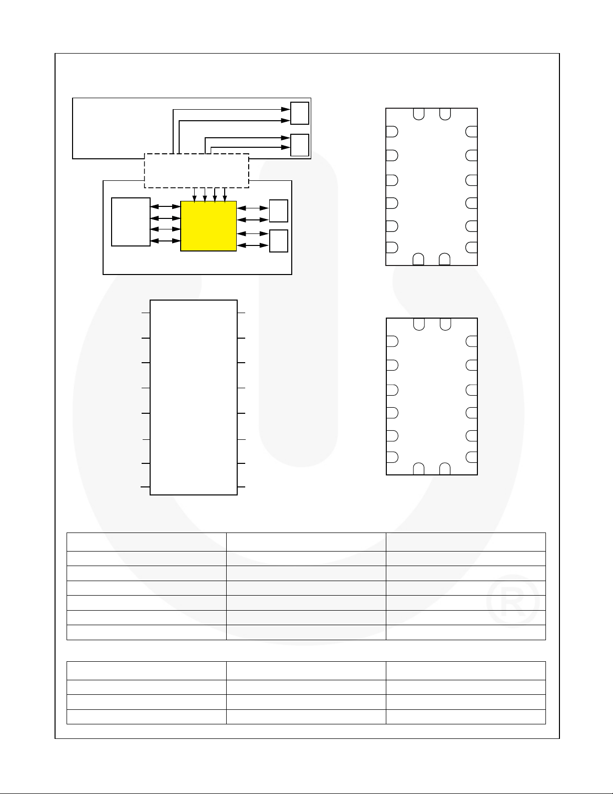
Logic Diagram Analog Symbol
D-
USB
Port
Docking Station
Docking Connector
D+
1B
2
1B
1A
1
3
2
4
D+
USB
D-
Port
FSUSB22 — Low-Power, 2-Port, High-Speed USB 2.0 (480Mbps) Switch
V
S
CC
16
1
15
/OE
4B
14
1
4B
13
2
USB 2.0
Host
Controller
D+
D-
D+
D-
FSUSB22
Notebook Computer
Figure 1. Logic Diagram
1
S
2
1B
1
3
1B
2
4
1A
5
2B
1
6
2B
2
7
2A
GND
8
D+
USB
Port
D-
D+
USB
D-
Port
V
16
CC
/OE
15
4B
14
1
4B
13
2
4A
12
3B
11
1
3B
10
2
3A
9
2B
2B
2A
5
1
6
2
7
8
12
11
10
9
GND 3A
Figure 2. Analog Symbol
V
S
CC
116
1B
1B
2B
2B
1A
2A
2
1
3
2
4
5
1
6
2
7
8
GND 3A
15
14
13
12
11
10
9
4A
3B
3B
/OE
4B
4B
4A
3B
3B
1
2
1
2
1
2
Figure 3. QSOP and TSSOP Pin Configuration Figure 4. Pad Assignment for DQFN
Pin Descriptions
Pin # Pin Names Description
1 S Select Input
2,3,5,6,10,11,13,14 1B1,1B2, 2B1,2B2,3B2,3B1,4B2,4B1 Bus B
8 GND Ground
4,7,9,12 1A,2A,3A,4A Bus A
15 /OE Bus Switch Enable
16 VCC Supply Voltage
Truth Table
S OE Function
Don’t Care HIGH Disconnect
LOW LOW A=B1
HIGH LOW A=B2
© 2005 Fairchild Semiconductor Corporation www.fairchildsemi.com
FSUSB22 • Rev. 1.0.3 2

FSUSB22 — Low-Power, 2-Port, High-Speed USB 2.0 (480Mbps) Switch
Absolute Maximum Ratings
Stresses exceeding the absolute maximum ratings may damage the device. The device may not function or be
operable above the recommended operating conditions and stressing the parts to these levels is not recommended.
In addition, extended exposure to stresses above the recommended operating conditions may affect device
reliability. The absolute maximum ratings are stress ratings only.
Symbol Parameter Min. Max. Unit
VCC Supply Voltage -0.5 4.6 V
VS DC Switch Voltage -0.5 VCC + 0.05 V
VIN DC Input Voltage
IIK DC Input Diode Current, VIN<0V -50 mA
I
DC Output Sink Current 128 mA
OUT
I
/ I
CC
DC V
GND
T
Storage Temperature Range -65 +150 °C
STG
/ GND Current ±100 mA
CC
ESD Human Body Model, JESD22-A114 4 kV
Note:
1. The input and output negative voltage ratings may be exceeded if the input and output diode current ratings are
observed.
(1)
-0.5 4.6 V
Recommended Operating Conditions
The Recommended Operating Conditions table defines the conditions for actual device operation. Recommended
operating conditions are specified to ensure optimal performance to the datasheet specifications. Fairchild does not
recommend exceeding them or designing to Absolute Maximum Ratings.
Symbol Parameter Min. Max. Unit
VCC Power Supply Operating 3.0 3.6 V
VIN Input Voltage 0 VCC V
V
Output Voltage 0 VCC V
OUT
tr, tf Input Rise and Fall Time
Switch Control Input
Switch I/O 0 DC
TA Operating Temperature, Free Air -40 +85 °C
Note:
2. Unused control inputs must be held HIGH or LOW. They may not float.
(2)
0 5
ns/V
© 2005 Fairchild Semiconductor Corporation www.fairchildsemi.com
FSUSB22 • Rev. 1.0.3 3

DC Electrical Characteristics
Typical values are at V
= 3.0V and TA = 25°C.
CC
FSUSB22 — Low-Power, 2-Port, High-Speed USB 2.0 (480Mbps) Switch
Symbol Parameter Conditions VCC (V)
TA=-40 to +85°C
Min. Typ. Max.
VIK Clamp Diode Voltage I
VIH High-Level Input Voltage 3.0 to 3.6 2.0 V
VIL Low-Level Input Voltage 3.0 to 3.6 0.8 V
IIN Input Leakage Current
I
OFF
RON Switch On Resistance
ΔRON
R
FLAT(ON)
Off-state Leakage
Current
Delta R
ON
On Resistance Flatness
(3)
ICC Quiescent Supply Current
Notes:
3. Measured by the voltage drop between the A and B pins at the indicated current through the switch. On
resistance is determined by the lower of the voltages on the A or B pins.
4. Flatness is defines as the difference between the maximum and the minimum value on resistance over the
specified range of conditions.
= -18mA 3.0 -1.2 V
IN
0 ≤ VIN ≤ 3.6V
0 ≤ A, B ≤ VCC
3.6 ±1.0 µA
3.6 ±1.0 µA
VIN = 0.8V, ION = 8mA 3.0 5 7
V
= 3.0V, ION = 8mA 3.0 4.5 6.5
IN
VIN = 0.8V, VIN = 0V - 1.5,
I
= 8mA
ON
(4)
I
= 8mA 3.0 1
OUT
VIN = VCC or GND,
I
= 0
OUT
3.0 0.3
3.6 1 µA
Units
Ω
Ω
Ω
© 2005 Fairchild Semiconductor Corporation www.fairchildsemi.com
FSUSB22 • Rev. 1.0.3 4
 Loading...