FSUSB11
Low-Power Full-Speed USB (12Mbps) Switch
FSUSB11 Low-Power Full-Speed USB (12Mbps) Switch
October 2006
Features
■ Space saving MicroPak™ Pb-free packaging
(1.6 x 2.1mm)
■ USB 1.1 signal switching compliant
■ -3db bandwidth: >350MHz
■ Maximum 1.15Ω R
and 4Ω for 2.7V supply
■ 0.3Ω maximum R
■ Broad V
■ Fast turn-on and turn-off time
■ Break-before-make enable circuitry
■ Over-voltage tolerant, TTL-compatible control input
operating range: 1.65V to 5.5V
CC
at 4.5V V
ON
flatness for +5V supply
ON
CC
Description
The FSUSB11 is a high-performance, dual Single-Pole
Double-Throw (SPDT) switch designed for switching
USB 1.1 signals. The device features ultra-low on resistance (R
2.7V supply. High bandwidth and ultra low (R
this switch able to pass both USB low- and full-speed
signal with minimum signal distortion. The device is fabricated with sub-micron CMOS technology to achieve fast
switching speeds and designed for break-before-make
operation. The select input is TTL-level compatible.
) of 1.15Ω maximum at 4.5V VCC and 4.3Ω at
ON
ON
) make
Applications
■ Cell Phone
■ PDS
■ Digital Camera
■ Notebook
Ordering Information
Top
Part Number Package
FSUSB11L10X 10-Lead MicroPak, 1.6 x 2.1mm ET Yes 5K units on tape and reel
FSUSB11MTCX 14-Lead Thin Shrink Small Outline Package
(TSSOP), JEDEC MO-153, 4.4mm Wide
FSUSB11MUX
(Preliminary)
Pb-Free package per JEDEC J-STD-020B.
10-Lead Molded Small Outline Package
(MSOP), JEDEC MO-187, 3.0mm
Mark
FSUSB11 Yes 2500 units on tape andreel
FSUSB11 Yes 3K units on tape and reel
Pb-
Free Packing Method
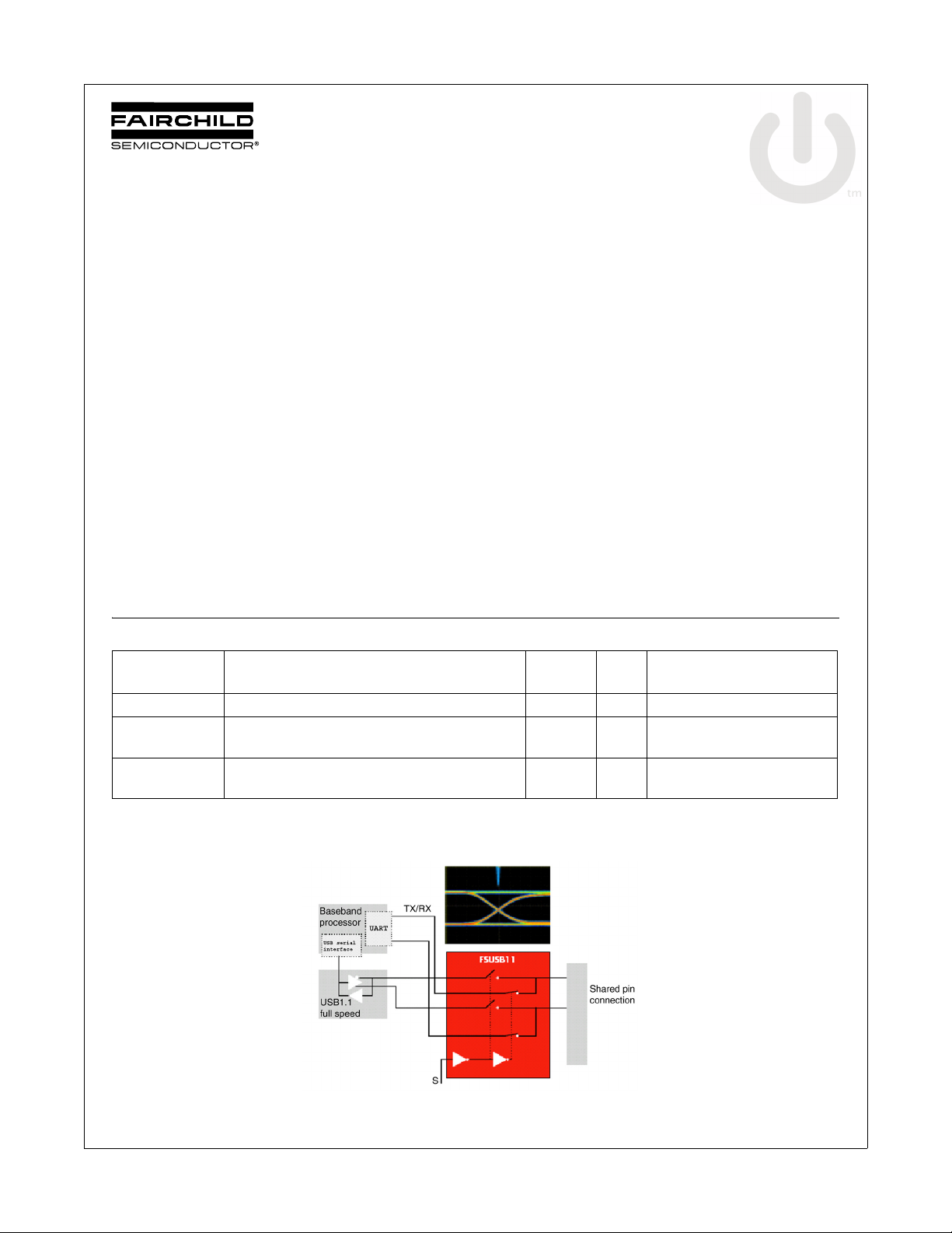
Block Diagram
MicroPak™ is a trademark of Fairchild Semiconductor Corporation.
© 2005 Fairchild Semiconductor Corporation www.fairchildsemi.com
FSUSB11 Rev. 1.0.2

Connection Diagrams
V
FSUSB11 Low-Power Full-Speed USB (12Mbps) Switch
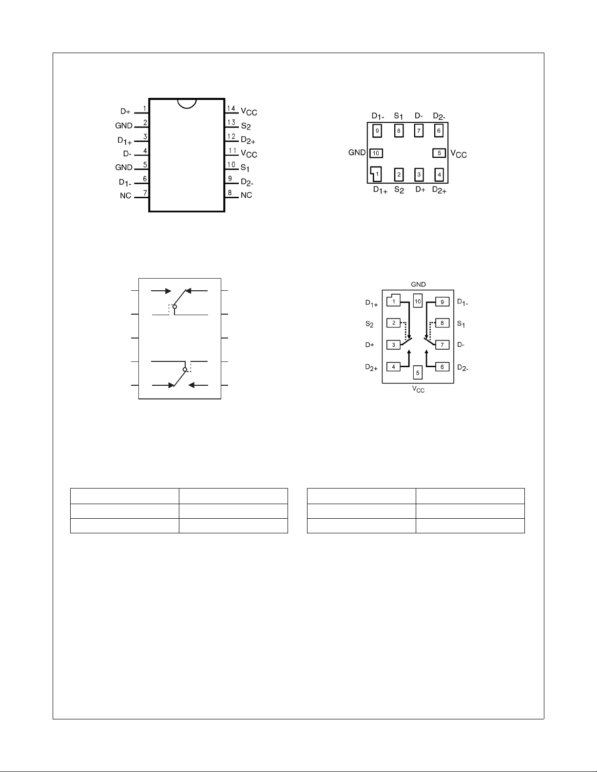
Figure 1. Pin Assingments for TSSOP
Figure 2. Pad Assignments for Micropak
(Top View)
Analog Symbols
D2-
1
S1
2
3
CC
D+
4
D
5
1+
Figure 3. Pin Assignments for MSOP
(Top Through View)
D1-
10
D-
9
GND
8
S2
7
D
6
2+
Figure 4. Analog Symbols
(Top Through View)
Truth Table Pin Desciption
Control Imputs Function
Low Logic Level D1 Connected to D+/D-
High Logic Level D
Connected to D+/D-
2
Pin names Function
D,D1,D
2
S Control Imput
(Top View)
Data Ports
© 2005 Fairchild Semiconductor Corporation www.fairchildsemi.com
FSUSB11 Rev. 1.0.2
2

Absolute Maximum Ratings
The “Absolute Maximum Ratings” are those values beyond which the safety of the device cannot be guaranteed. The
device should not be operated at these limits. The parametric values defined in the Electrical Characteristics tables
are not guaranteed at the absolute maximum ratings. The “Recommended Operating Conditions” table defines the
conditions for actual device operation.
Symbol Parameter Min. Max. Unit
(1)
(1)
-0.5 +6.0 V
-0.5 VCC to +0.5 V
400
V
CC
V
S
V
IN
I
IK
I
SW
I
SWPEAK
Supply Voltage
Switch Voltage
Input Voltage -0.5 +6.0 V
Input Diode Current -50 mA
Switch Current 200 mA
Peak Switch Current (Pulsed at 1ms Duration,<10% Duty
Cycle)
T
STG
T
J
T
L
Storage Temperature Range -65 +150 °C
Maximum Junction Temperature +150 °C
Lead Temperature (Soldering, 10 seconds) +260 °C
ESD Human Body Model 8000 V
Notes:
1. The input and output negative voltage ratings may be exceeded if the input and output diode current ratings are
observed.
FSUSB11 Low-Power Full-Speed USB (12Mbps) Switch
Recommended Operating Conditions
Symbol Parameter Min. Max. Unit
V
CC
V
IN
V
SW
T
A
Notes:
2. Unused inputs must be held HIGH or LOW. They may not float.
Supply Voltage 1.65 5.50 V
Control Input Voltage
Switch Input Voltage 0 V
(2)
0VCCVCC
CC
Operating Temperature -40 +85 °C
V
CC
© 2005 Fairchild Semiconductor Corporation www.fairchildsemi.com
FSUSB11 Rev. 1.0.2
3

DC Electrical Characteristics
All typical values are at 25°C unless otherwise specified.
Symbol Parameter Conditions
V
I
NO(OFF)
I
NC(OFF)
I
A(ON)
R
ΔR
R
FLAT(ON)
I
Input Voltage High
IH
V
Input Voltage Low
IL
I
Control Input Leakage VIN = 0V to V
IN
,
Off-Leakage Current of
Port D1 and D
2
On-Leakage Current of
Port D
Switch On Resistance
MicroPak
ON
Switch On Resistance
TSSOP
(3)
(3)
On Resistance Matching
Between Channels
MicroPak
ON
On Resistance Matching
Between Channels
TSSOP
(4)
(4)
On Resistance Flatness
Quiescent Supply Current
CC
CC
A = 1V, 4.5V, B0 or B1 =
1V, 4.5V
A = 1V, 4.5V,B0 or B1 =
1V, 4.5V or Floating
I
= 100mA, D1 or D2
OUT
= 1.5V
= 100 mA, D1 or D2
I
OUT
= 3.5V
I
= 100mA, D1 or D2
OUT
= 1.5V
I
= 100mA, D1 or D2
OUT
= 3.5V
I
= 100mA, D1 or D2
OUT
= 3.5V
I
= 100mA, D1 or D2
OUT
= 3.5V
I
= 100mA, D1 or D2
OUT
= 0V, 0.75V, 1.5V
(5)
I
= 100mA,
OUT
or B1 = 0V, 1V, 2V
B
0
= 0V or VCC,
V
IN
I
= 0V
OUT
= -40 °C
T
A
V
CC
TA = + 25 C°
to +85 C°
2.7 to 3.6 2.0
4.5 to 5.5 2.4
2.7 to 3.6 0.6
4.5 to 5.5 0.8
2.7 to 3.6 -1.0 1.0
4.5 to 5.5 -1.0 1.0
5.5 -50.0 50.0 -100 100
5.5 50.0 50.0 -100 100
2.7 2.6 4.0 4.3
4.50 0.95 1.15 1.30
2.7 2.8 4.5
4.5 1.5 3.0
4.50 0.06 0.12 0.15
4.50 0.07 0.30
2.7 1.4
4.5 0.2 0.3 0.4
3.6 0.1 0.5 1.0
5.5 0.1 0.5 1.0
FSUSB11 Low-Power Full-Speed USB (12Mbps) Switch
Units(V) Min. Typ. Max. Min. Max.
V
V
µA
nA
nA
Ω
Ω
Ω
µA
Notes:
3. On resistance is determined by the voltage drop between D and D
4. ΔR
ON
= R
ONmax
- R
measured at identical VCC, temperature, and voltage.
ONmin
pins at the indicated current through the switch.
n
5. Flatness is defined as the difference between the maximum and minimum value of on resistance over the specified
range of conditions.
© 2006 Fairchild Semiconductor Corporation www.fairchildsemi.com
FSUSB11 Rev. 1.0.2
4

AC Electrical Characteristics (Continued)
All typical values are at 25°C unless otherwise specified.
Symbol Parameter Conditions
or D2 = 1.5V, RL =
D
1
t
Turn-ON Time
ON
t
t
Turn-OFF Time
OFF
Break-Before-Make
BBM
Time
Q Charge Injection
OIRR OFF-Isolation f = 1MHz, RL = 50Ω
X
Crosstalk f = 1MHz, RL = 50Ω
talk
BW -3db Bandwidth R
50Ω, CL = 35 pF
D
or D2 = 3.0V, RL =
1
50Ω, CL = 35 pF
D1 or D2 = 1.5V, RL =
50Ω, C
D
or D2 = 3.0V, RL =
1
= 35 pF
L
50Ω, CL = 35 pF
D
or D2 = 1.5V, RL =
1
50Ω, CL = 35 pF
D
or D2 = 3.0V, RL =
1
50Ω, C
= 1.0 nF, V
C
L
= 35 pF
L
= 0V, 2.7 to 3.6 20.0
GEN
R
= 0Ω 4.5 to 5.5 10.0
GEN
= 50Ω
L
= -40 C°
T
A
V
CC
TA = +25 C°
(V) Min. Typ. Max. Min. Max. Number
to +85 C°
Units
Figure
2.7 to 3.6 50.0 60.0
4.5 to 5.5 35.0 40.0
ns Figure 5
2.7 to 3.6 20.0 30.0
4.5 to 5.5 15.0 20.0
ns Figure 5
2.7 to 3.6 1.0
4.5 to 5.5 20.0 1.0
ns Figure 6
pC Figure 8
2.7 to 3.6 -70.0
4.5 to 5.5 -70.0
2.7 to 3.6 -75.0
4.5 to 5.5 -75.0
2.7 to 3.6 350
4.5 to 5.5 350
dB Figure 7
dB Figure 7
MHz Figure 10
FSUSB11 Low-Power Full-Speed USB (12Mbps) Switch
USB Related AC Electrical Characteristics
All typical values are at 25°C unless otherwise specified.
Symbol Parameter Conditions
= 39, CL = 50 pF,
R
t
SKEW
t
M
t
Skew
Rising/Fall Time Mismatch
Total Jitter
J
S
tR = tF = 12ns at 12Mbps
(Duty Cycle = 50%)
= 39, CL = 50 pF, tR = tF =
R
S
12ns at 12Mbps (PRBS = 2
Capacitance
Symbol Parameter Conditions
C
C
C
Control Pin Input Capacitance f = 1MHz 0.0 3.5 pF Figure 9
IN
OFFDn
ON
Port OFF Capacitance f = 1MHz 4.5 12.0 pF Figure 9
D Port ON Capacitance f = 1MHz 4.5 40.0 pF Figure 9
V
CC
TA = +25° C
(V) Min.Typ.Min. Number
2.7 to 3.6 0.15
4.5 to 5.5 0.15
2.7 to 3.6 10.0
4.5 to 5.5 10.0
2.7 to 3.6 1.7
15
1)
4.5 to 5.5 1.6
V
CC
TA = +25 C°
(V) Min. Typ. Max. Number
Figure
Units
ns Figure 11
% Figure 12
ns Figure 11
Figure
Units
© 2005 Fairchild Semiconductor Corporation www.fairchildsemi.com
FSUSB11 Rev. 1.0.2
5

AC Loading and Waveforms
FSUSB11 Low-Power Full-Speed USB (12Mbps) Switch
CL includes Fixture and Stray Capacitance
Includes Fixture and Stray Capacitance
C
L
Logic Input Waveforms Inverted for Switches that
have the Opposite Logic Sense
Figure 5. Turn-On/Turn-Off Timing
Figure 6. Break-Before-Make Timing
Figure 7. OFF Isolation and Crosstalk
© 2006 Fairchild Semiconductor Corporation www.fairchildsemi.com
FSUSB11 Rev. 1.0.2
6

AC Loading and Waveforms (Continued)
FSUSB11 Low-Power Full-Speed USB (12Mbps) Switch
Figure 8. Charge Injection
Figure 9. ON / OFF Capacitance Measurement Setup
Q = ( ΔV
OUT
)(CL)
Figure 10. Bandwidth
Figure 11. Skew Test
Figure 12. Rise / Fall Time Mismatch Test
© 2006 Fairchild Semiconductor Corporation www.fairchildsemi.com
FSUSB11 Rev. 1.0.2
7

Tape and Reel Specification
Tape Format for Micropak 10
Package Tape Number Cavity Cover Tape
Designator Section Cavities Status Status
Leader (Start End) 125 (typ) Empty Sealed
L10X Carrier 5000 Filled Sealed
Trailer (Hub End) 75 (typ) Empty Sealed
FSUSB11 Low-Power Full-Speed USB (12Mbps) Switch
Reel Dimensions
Dimensions are in inches (millimeters) unless otherwise noted.
Tape Size A B C D N W1 W2 W3
7.0 0.059 0.512 0.795 2.165 0.331 + 0.059/-0.000 0.567 W1 +0.078/-0.039
(8mm)
© 2006 Fairchild Semiconductor Corporation www.fairchildsemi.com
FSUSB11 Rev. 1.0.2
(177.8) (1.50) (13.00) (20.20) (55.00) (8.40 + 1.50/-0.00) (14.40) (W1 +2.00/-1.00)
8

Tape Dimensions for MSOP
Dimensions are in millimeters (inches) unless otherwise specified.
FSUSB11 Low-Power Full-Speed USB (12Mbps) Switch
Reel Dimensions for MSOP
Dimensions are in inches (millimeters) unless otherwise specified.
Tape SizeABCDNW1W2W3
(12mm)
13
(330)
0.059
(1.5)
0.512
(13)
0.795
(20.2)
7.008
(178)
0.448
(12.4)
0.724
(18.4)
0.468-0.606
(11.9 -15.4)
© 2006 Fairchild Semiconductor Corporation www.fairchildsemi.com
FSUSB11 Rev. 1.0.2
9

Physical Dimension
Dimensions are in millimeters (inches) unless otherwise noted.
FSUSB11 Low-Power Full-Speed USB (12Mbps) Switch
Figure 13. Pb-Free 10-Lead MicroPak, 1.6 x 2.1mm
© 2006 Fairchild Semiconductor Corporation www.fairchildsemi.com
FSUSB11 Rev. 1.0.2
10

Physical Dimension (Continued)
Dimensions are in millimeters (inches) unless otherwise noted.
FSUSB11 Low-Power Full-Speed USB (12Mbps) Switch
Figure 14. 14-Lead Thin-Shrink Small Outline Package (TSSOP), JEDEC MO-153, 4.4mm Wide
© 2006 Fairchild Semiconductor Corporation www.fairchildsemi.com
FSUSB11 Rev. 1.0.2
11

Physical Dimension (Continued)
Dimensions are in millimeters (inches) unless otherwise noted.
FSUSB11 Low-Power Full-Speed USB (12Mbps) Switch
Figure 15. 10-Lead Molded Small Outline Package (MSOP), JEDEC MO-187, 3.0mm
© 2006 Fairchild Semiconductor Corporation www.fairchildsemi.com
FSUSB11 Rev. 1.0.2
12

FSUSB11 Low-Power Full-Speed USB (12Mbps) Switch
© 2005 Fairchild Semiconductor Corporation www.fairchildsemi.com
FSUSB11 Rev. 1.0.2
13
 Loading...