FSTD16211
24-Bit Bus Switch with Level Shifting
FSTD16211 24-Bit Bus Switch with Level Shifting
June 2000
Revised April 2005
General Description
The Fairchild Switch FSTD 16211 provides 24-bits of highspeed CMOS TTL-compatible bus switching. The low On
Resistance of the switch allows inputs to be connected to
outputs without adding propagation delay or generating
additional ground b ounce noise. A diode to V
integrated into the circuit to allow for level shifting between
5V inputs and 3.3V outputs.
The device is organ ized as a 12-bit or 24-bit b us switch.
When OE
nected to Port 1B. When OE
to Port 2B. Wh en OE
exists between the A and B Ports.
is LOW, the switch is ON and Port 1A is con-
1
is LOW, Port 2A is connected
2
is HIGH, a high impedance state
1/2
has been
CC
Features
■ 4
:
switch connection between two ports
■ Voltage level shifting
■ Minimal propagation delay through the switch
■ Low l
CC
■ Zero bounce in flow-through mode
■ Control inputs compatible with TTL level
■ Also packaged in plastic Fine-Pitch Ball Grid Array
(FBGA)
Ordering Code:
Order Number Package Number Package Description
FSTD16211G
(Note 1)(Note 2)
FSTD16211MTD
(Note 2)
Note 1: Ordering code “G” indicates Trays.
Note 2: Devices also available in Tape and Reel. Specify by appending the suffix let te r “X” to the ordering code.
BGA54A 54-Ball Fine-Pitch Ball Grid Array (FBGA), JEDEC MO-205, 5.5mm Wide
[TAPE and REEL]
MTD56 56-Lead Thin Shrink Small Outline Package (TSSOP), JEDEC MO-153, 6.1mm Wide
Logic Diagram
© 2005 Fairchild Semiconductor Corporation DS500313 www.fairchildsemi.com

Connection Diagrams
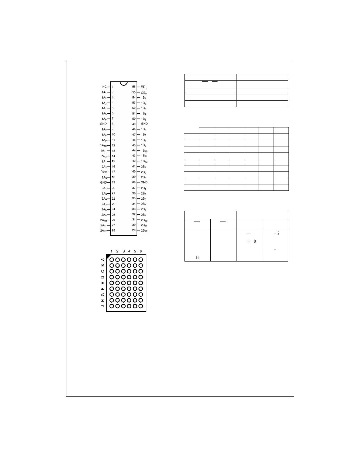
Pin Assignment for TSSOP
FSTD16211
Pin Assignment for FBGA
Pin Descriptions
Pin Name Description
OE
, OE
1
2
1A, 2A Bus A
1B, 2B Bus B
NC No Connect
Bus Switch Enables
Pin Assignment for FBGA
123456
A 1A21A1NC OE21B11B
B 1A41A31A7OE11B31B
C 1A61A5GND 1B71B51B
D 1A101A91A81B81B91B
E 1A121A112A12B11B111B
F 2A42A32A22B22B32B
G 2A62A5VCCGND 2B52B
H 2A82A72A92B92B72B
J 2A122A112A102B102B112B
Truth Table
Inputs Inputs/Outputs
OE
1
LL1A
LH1A
HLZ2A
HHZZ
OE
2
1A, 1B 2A, 2B
1B 2A 2B
1B Z
2
4
6
10
12
4
6
8
12
2B
(Top Thru View)
www.fairchildsemi.com 2

Absolute Maximum Ratings(Note 3) Recommended Operating
Supply Voltage (VCC)
DC Switch Voltage (V
) (Note 4)
S
DC Input Control Pin Voltage (V
DC Input Diode Current (l
DC Output (I
DC V
CC
) 128 mA
OUT
/GND Current (ICC/I
) V
IK
GND
Storage T emperature Range (T
0.5V to 7.0V
0.5V to 7.0V
)(Note 5)0.5V to 7.0V
IN
0V
IN
)
STG
)
65q
C to 150 qC
/
50 mA
100 mA
Conditions
Power Supply Operating (V
Input Voltage (V
Output Voltage (V
Input Rise and Fall Time (t
Switch Control Input 0 ns/V to 5 ns/V
Switch I/O 0 ns/V to DC
Free Air Operating Temperature (T
Note 3: The “Absolute Maximum Ratings” are those value s beyond which
the safety of the d evice cannot b e guaranteed . The device sh ould not be
operated at these lim its. The parametric values defin ed in the Electrical
Characteristics tables are not guaranteed at the absolute maximum rating.
The “Recomm ended O peratin g Con ditions ” table will defin e the condition s
for actual device operation.
is the voltage observed/applied at either A or B Ports across the
Note 4: V
S
switch.
Note 5: The input and output negative voltage ratings may be exceeded if
the input and ou t put diode current ratings ar e observed.
Note 6: Unused control inputs m ust b e held H IGH o r LOW. They may n ot
float.
(Note 6)
CC)
) 0V to 5.5V
IN
) 0V to 5.5V
OUT
, tf)
r
)-40 qC to 85 qC
A
4.5V to 5.5V
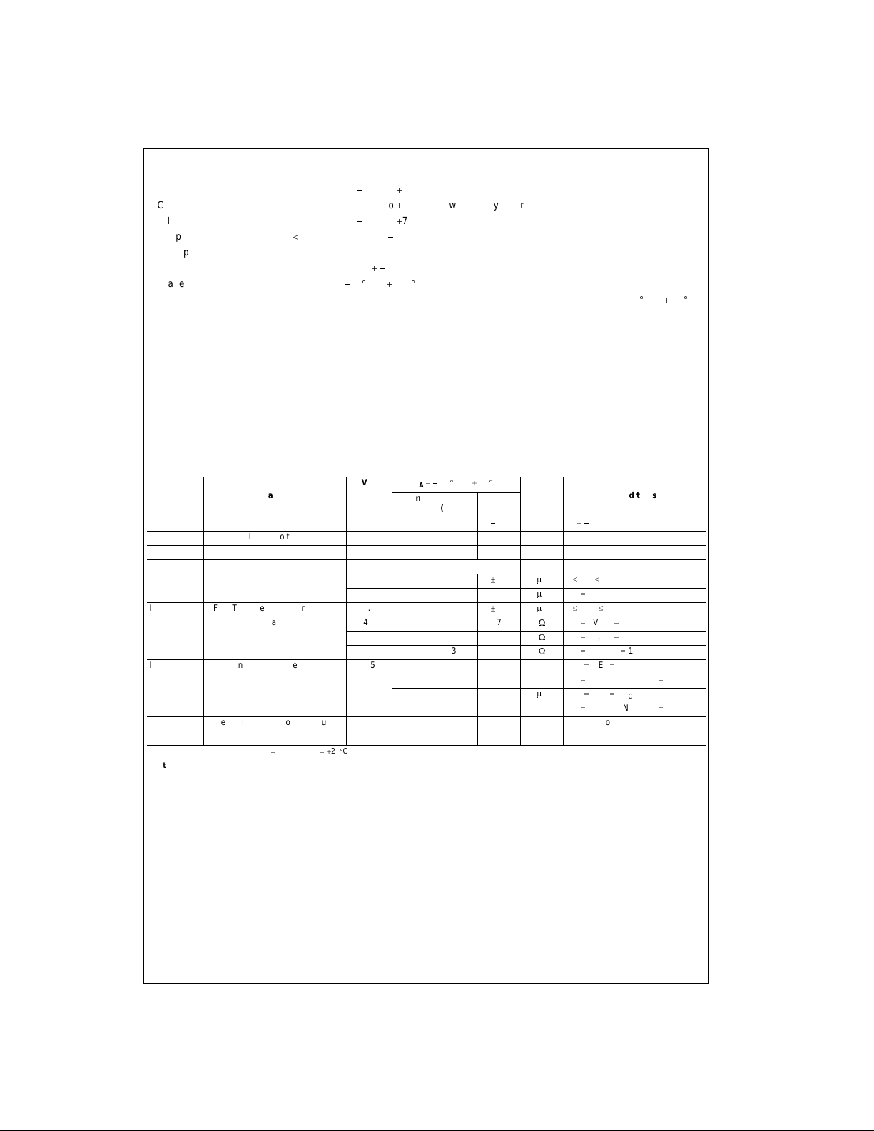
DC Electrical Characteristics
V
Symbol Parameter
V
IK
V
IH
V
IL
V
OH
I
I
I
OZ
R
ON
I
CC
I
CCT
Note 7: Typical values are at VCC 5.0V and T
Note 8: Measured by the voltage drop between A and B pins at the indicated cu rrent through the switc h. On Resistance is determ ined by the lower of the
voltages on the two (A or B ) pins.
Clamp Diode Voltage 4.5
HIGH Level Input Voltage 4.5–5.5 2.0 V
LOW Level Input Voltage 4.5–5.5 0.8 V
HIGH Level 4.5–5.5 See Figure 3 V
Input Leakage Current 5.5
OFF-STATE Leakage Current 5.5
Switch On Resistance 4.5 4 7
(Note 8) 4.5 4 7
Quiescent Supply Current 5.5 1.5 mA OE1 OE2 GND
Increase in I
per Control Input 5.5 2.5 mA One Control Input at 3.4V
CC
25q
A
CC
(V) Min Typ
010
4.5 35 50
C
TA 40 qC to 85 qC
(Note 7)
Units Conditions
Max
1.2 V IIN 18 mA
r
1.0
P
A0 d VIN d 5.5V
5.5V
P
AV
r
1.0
10
IN
P
A0 d A, B d V
:
VIN 0V, IIN 64 mA
0V, IIN 30 mA
:
V
IN
:
VIN 2.4V, IIN 15 mA
VCC or GND, I
V
IN
P
AOE1 OE2 V
VIN VCC or GND, I
Other Control Inputs at VCC or GND
CC
0
OUT
CC
0
OUT
FSTD16211
3 www.fairchildsemi.com
 Loading...