

Fairchild FST3253 service manual
查询FST3253供应商
FST3253
Dual 4:1 Multiplexer/Demultiplexer Bus Switch
FST3253 Dual 4:1 Multiplexer/Demultiplexer Bus Switch
September 1997
Revised December 1999
General Description
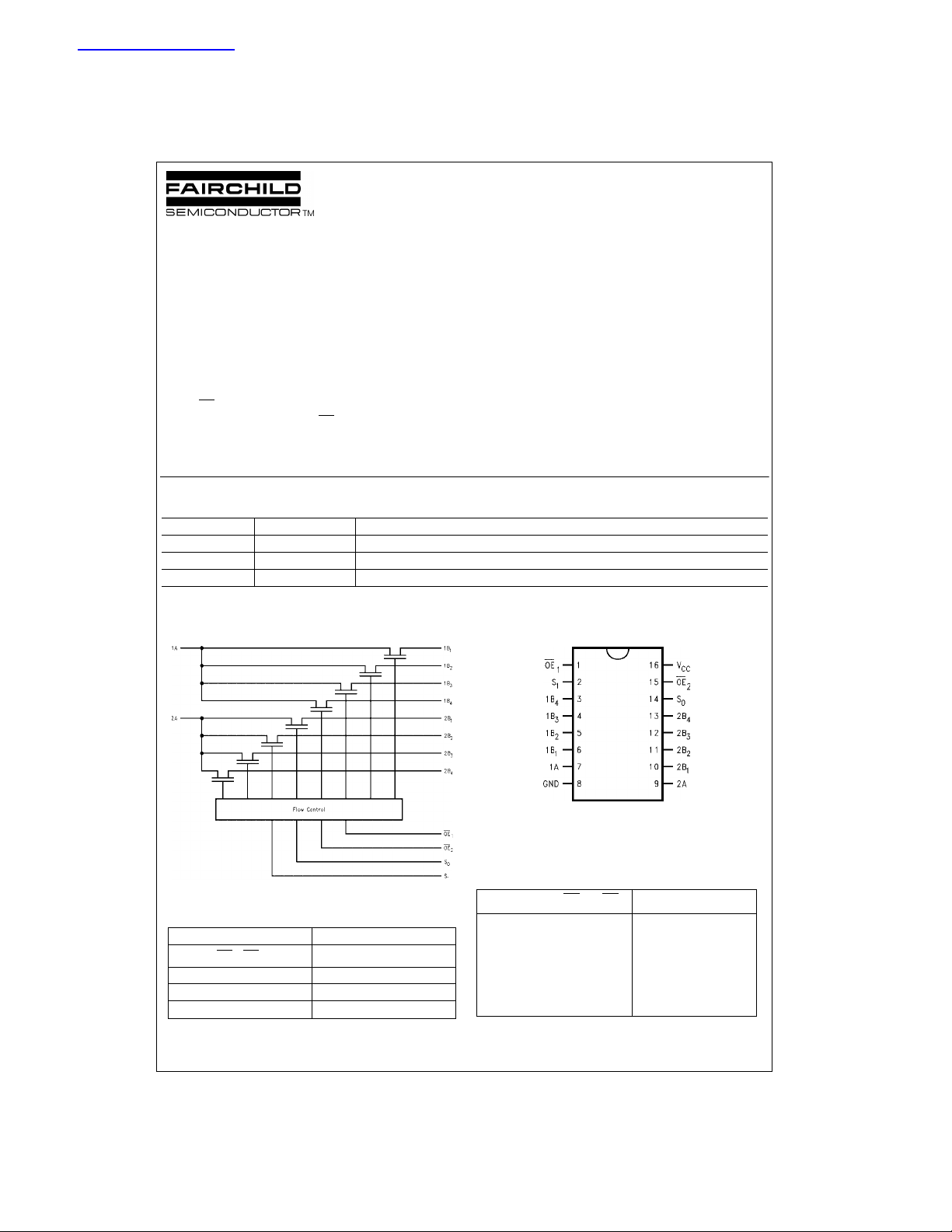
The Fairchild Switch FST3253 is a dual 4:1 high-speed
CMOS TTL-compatible multiplexer/demultiplexer bus
switch. The low on resistance of the switch allows inputs to
be connected to outputs wi thout a dding pr opagation delay
or generating additional ground bounce noise.
When OE
selected B Port output. When OE
OPEN and a high-impedance sta te exist s between the two
ports.
is LOW, S0 and S1 connect the A Port to the
is HIGH, the switch is
Features
■ 4Ω switch connection between two ports.
■ Minimal propagation delay through the switch.
■ Low l
■ Zero bounce in flow-through mode.
■ Control inputs compatible with TTL level.
.
CC
Ordering Code:
Order Number Package Number Package Description
FST3253M M16A 16-Lead Small Outline Integrated Circuit (SOIC), JEDEC MS-012, 0.150 Narrow
FST3253QSC MQA16 16-Lead Quarter Size Outline Package (QSOP), JEDEC MO-137, 0.150 Wide
FST3253MTC MTC16 16-Lead Thin Shrink Small Outline Package (TSSOP), JEDEC MO-153, 4.4mm Wide
Device also available in Tape and Reel. Specify by appending suffix letter “X” to the or dering code.
Logic Diagram
Connection Diagram
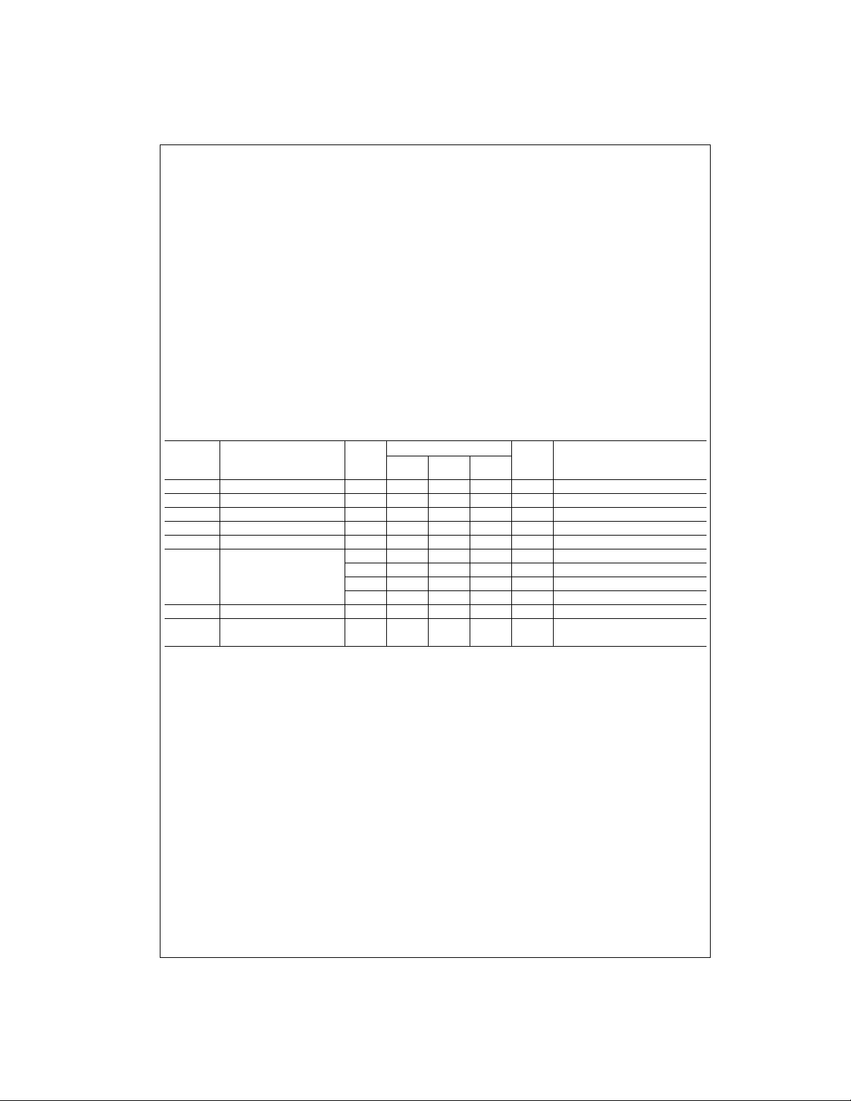
Truth Table
S
S0OE1OE
Pin Descriptions
Pin Name Description
OE
, OE
1
2
S
, S
0
1
ABus A
, B2, B3, B
B
1
© 1999 Fairchild Semiconductor Corporation DS500058 www.fairchildsemi.com
4
Bus Switch Enables
Select Inputs
Bus B
1
X X H X Disconnect 1A
X X X H Disconnect 2A
LLLL A = B
LHLL A = B
HLLL A = B
HHL L A = B
2
Function
1
2
3
4
Absolute Maximum Ratings(Note 1) Recommended Operating
Supply Voltage (VCC) −0.5V to +7.0V
DC Switch Voltage (V
FST3253
DC Input Voltage (V
DC Input Diode Current (l
DC Output (I
DC V
OUT
/GND Current (ICC/I
CC
Storage Temperature Range (T
) −0.5V to +7.0V
S
)(Note 2) −0.5V to +7.0V
IN
) VIN<0V −50mA
IK
) Sink Current 128mA
) +/− 100mA
GND
) −65°C to +150 °C
STG
Conditions
Power Supply Operating (V
Input Voltage (V
Output Voltage (V
Input Rise and Fall Time (t
Switch Control Input 0ns/V to 5ns/V
Switch I/O 0ns/V to DC
Free Air Operating Temperature (T
Note 1: The Absolute Maximum Ratings are those values beyond which
the safety of the d evice cannot be guaranteed. The device sh ould not be
operated at these limit s. The parametric values defin ed in the Electrical
Characteristics tables are not guaranteed at the absolute maximum rating.
The Recommende d Opera ting Condit ions table s will de fine the co nditions
for actual device operation.
Note 2: The input and output ne gative vo ltage ra tings may be excee ded if
the input and output diode current ratings are observed.
Note 3: Unused control inputs must be held HIGH or LOW. They may not
float.
(Note 3)
CC)
)0V to 5.5V
IN
)0V to 5.5V
OUT
, tf)
r
) −40 °C to −85 °C
A
DC Electrical Characteristics
= −40 °C to +85 °C
T
V
Symbol Parameter
V
IK
V
IH
V
IL
I
I
I
OZ
R
ON
I
CC
∆ I
CC
Note 4: Typi c al values are at VCC = 5.0V and TA = +25°C
Note 5: Measured by the volta ge drop between A an d B pins at the indicated c urrent through the switch. On resistance is determined by the lower of the
voltages on the two (A or B) pins.
Clamp Diode Voltage 4.5 −1.2 V IIN = −18mA
High Level Input Voltage 4.0–5.5 2.0 V
Low Level Input Voltage 4.0–5.5 0.8 V
Input Leakage Current 5.5 ±1.0 µA0≤ VIN ≤5.5V
OFF-STATE Leakage Current 5.5 ±1.0 µA0 ≤A, B ≤V
Switch On Resistance 4.5 4 7 Ω VIN = 0V, IIN = 64mA
(Note 5) 4.5 4 7 Ω V
Quiescent Supply Current 5.5 3 µAVIN = VCC or GND, I
Increase in I
per Input 5.5 2.5 mA One input at 3.4V
CC
CC
(V)
4.5 8 15 Ω V
4.0 11 20 Ω VIN = 2.4V, IIN = 15mA
Min
A
Typ
(Note 4)
Units Conditions
Max
Other inputs at VCC or GND
CC
= 0V, IIN = 30mA
IN
= 2.4V, IIN = 15mA
IN
OUT
4.0V to 5.5V
= 0
www.fairchildsemi.com 2
 Loading...