FSQ500N
Green Mode Fairchild Power Switch (FPS™)
FSQ500N — Green Mode Fairchild Power Switch (FPS™)
October 2009
Features
Single-Chip 700V SenseFET Power Switch
Precision Fixed Operating Frequency: 130kHz
No-Load Consumption 250mW at 265V
Burst Mode
AC
with
Internal Startup Switch
Soft-Start Time Tuned by External Capacitor
Under-Voltage Lockout (UVLO) with Hysteresis
Pulse-by-Pulse Current Limit
Overload Protection (OLP) and Internal Thermal
Shutdown Function (TSD) with Hysteresis
Auto-Restart Mode
No Need for Auxiliary Bias Winding
Applications
STB and DSL Power Supply
Home Appliance, IH Cooker, Auxiliary Power
Supply
Related Resources
AN-4137-Design Guidelines for Off-line Flyback
Converters using FPS
AN-4141-Troubleshooting and Design Tips for
Fairchild Power Switch (FPStm) Flyback
Applications
AN-4147-Design Guidelines for RCD Snubber of
Flyback
AN6075- (Flyback) -AN-6075-Compact Green-
Mode Adapter Using FSQ500L for Low Cost
Description
The FSQ500N is specially designed for low cost, small
set-top box, DSL, home appliance auxiliary power
supplies. This device combines a current-mode Pulse
Width Modulator (PWM) with a SenseFET. The
integrated PWM controller features include: a fixed
oscillator, Under-Voltage Lockout (UVLO) protection,
Overload Protection (OLP), Leading-Edge Blanking
(LEB), an optimized gate turn-on/turn-off driver,
Thermal Shutdown (TSD) protection with hysteresis,
and temperature-compensated precision-current
sources for loop compensation. When compared to a
linear power supply, the FSQ500N reduces total size
and weight, while increasing efficiency, productivity, and
system reliability. This device provides a basic platform
for cost-effective flyback converters.
(1)
Maximum Output Power
230VAC ± 15%
Adapter
Notes:
1. The junction temperature can limit the maximum
2. 230V
3. Typical continuous power in a non-ventilated
4. Maximum practical continuous power in an open
(3)
4.0W 6.5W 3.5W 5.5W
output power.
or 100/115VAC with doubler.
AC
enclosed adapter measured at 50°C ambient.
frame design at 50°C ambient.
(2)
85-265VAC
Open
Frame
Adapter
(4)
Open
Frame
(4)
(3)
Ordering Information
Part Number
FSQ500N -40°C to +85°C RoHS
For Fairchild’s definition of Ec o S tatus, please visit: http://www.fairchildsemi.com/company/green/rohs_green.html.
© 2009 Fairchild Semiconductor Corporation www.fairchildsemi.com
FSQ500N • Rev. 1.0.0
Operating
Temperature Range
Eco
Status
Package
8-Lead, Molded Dual Inline Package
(MDIP), JEDEC MS-001, .300 Inch Wide
Packing
Method
Rail

Application Circuit Diagram
AC
IN
FSQ500N — Green Mode Fairchild Power Switch (FPS™)
DC
OUT
Drain
PWM
Internal Block Diagram
V
FB
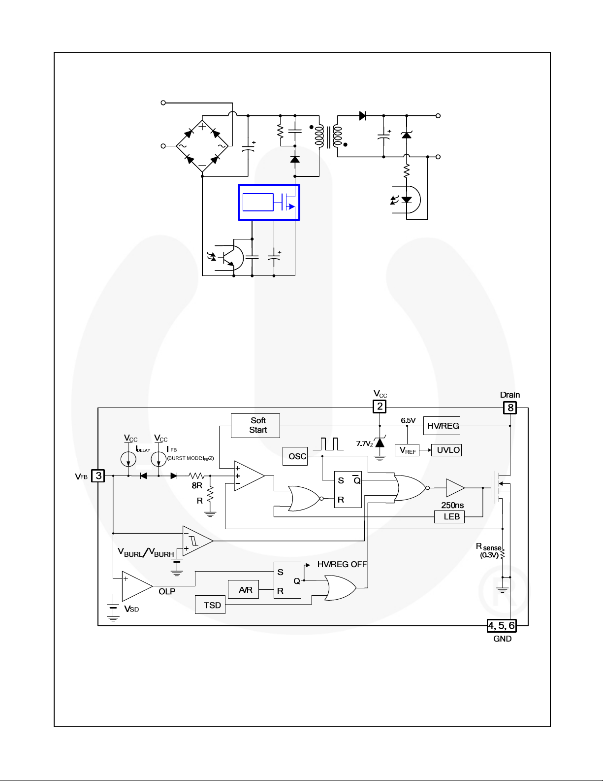
Figure 1. Typical Application Circuit
GND
V
CC
Figure 2. Internal Block Diagram
© 2009 Fairchild Semiconductor Corporation www.fairchildsemi.com
FSQ500N • Rev. 1.0.0 2

Pin Configuration
Pin Definitions
NC
Drain
V
CC
V
FB
8-DIP
NC
GND
GNDGND
Figure 3. Package / Pin Diagram
FSQ500N — Green Mode Fairchild Power Switch (FPS™)
Pin # Name Description
1 NC No connection
This pin is connected to a storage capacitor. A high-voltage regulator connected between pin 8
(V
) and this pin provides the supply voltage to the FSQ500N at startup and when switching
2 VCC
3 VFB
4, 5, 6 GND This pin is the control ground and the SenseFET source.
7 NC No connection
8 Drain High-voltage power SenseFET drain connection
STR
during normal operation. The FSQ500N eliminates the need for auxiliary bias winding and
associated external components.
This pin is internally connected to the non-inverting input of the PWM comparator. The collector of
an opto-coupler is typically tied to this pin. For stable operation, a capacitor should be placed
between this pin and GND. If the voltage of this pin reaches 4.5V, the overload protection triggers,
which shuts down the FPS.
© 2009 Fairchild Semiconductor Corporation www.fairchildsemi.com
FSQ500N • Rev. 1.0.0 3

Absolute Maximum Ratings
Stresses exceeding the absolute maximum ratings may damage the device. The device may not function or be
operable above the recommended operating conditions and stressing the parts to these levels is not recommended.
In addition, extended exposure to stresses above the recommended operating conditions may affect device
reliability. The absolute maximum ratings are stress ratings only.
Symbol Parameter Min. Max. Unit
VDS Drain Pin Voltage
VCC Supply Voltage 10 V
V
Feedback Voltage Range -0.3 VCC V
FB
PD Total Power Dissipation 1.42 W
IDM Drain Current Pulsed
TJ Operating Junction Temperature -40 +150
T
Storage Temperature -55 +150
STG
ESD
(7)
Human Body Model, JESD22-A114 2.5
Charged Device Model, JESD22-C101 2
Notes:
5. LDMOS available drain voltage is -0.3V ~ 700V.
6. Repetitive rating: pulse width is limited by maximum junction temperature.
7. Meet JEDEC Standards JESD 22-A114 and JESD 22-C101
(5)
700 V
(6)
0.41 A
°C
°C
KV
FSQ500N — Green Mode Fairchild Power Switch (FPS™)
Thermal Impedance
Symbol Parameter Value Unit
(8)(9)
θ
Junction-to-Ambient Thermal Resistance 88 °C/W
JA
(8)(10)
θ
Note:
8. All items are tested with the standards JESD 51-2 and JESD 51-10 (DIP Package).
9. θ
10. θ
Junction-to-Case Thermal Resistance 19 °C/W
JC
Free-standing, with no heat-sink, under natural convection.
JA
, Junction to lead thermal characteristics under ΘJA test condition. TC is measured on the source #7 pin
JC
closed to plastic interface for Θ
thermo couple is mounted on soldering.
JA
© 2009 Fairchild Semiconductor Corporation www.fairchildsemi.com
FSQ500N • Rev. 1.0.0 4
 Loading...