Fairchild FSQ0765RQ service manual

FSQ0765RQ
Green-Mode Fairchild Power Switch (FPS™) for
FSQ0765RQ — Green-Mode Farichild Power Switch (FPS™) for Quasi-Resonant Operation
April 2009
Quasi-Resonant Operation -
Features
! Optimized for Quasi-Resonant Converter (QRC)
! Low EMI through Variable Frequency Control and AVS
(Alternating Valley Switching)
! High-Efficiency through Minimum Voltage Switching
! Narrow Frequency Variation Range over Wide Load
and Input Voltage Variation
! Advanced Burst-Mode Operation for Low Standby
Power Consumption
! Simple Scheme for Sync Voltage Detection
! Pulse-by-Pulse Current Limit
! Various Protection functions: Overload Protection
(OLP), Over-Voltage Protection (OVP), Abnormal
Over-Current Protection (AOCP), Internal Thermal
Shutdown (TSD) with Hysteresis, Output Short
Protection (OSP)
! Under-Voltage Lockout (UVLO) with Hysteresis
! Internal Startup Circuit
! Internal High-Voltage Sense FET (650V)
! Built-in Soft-Start (17.5ms)
Applications
! Power Supply for LCD TV and Monitor, VCR, SVR,
STB, and DVD & DVD Recorder
! Adapter
Low EMI and High Efficiency
Description
A Quasi-Resonant Converter (QRC) generally shows
lower EMI and higher power conversion efficiency than a
conventional hard-switched converter with a fixed
switching frequency. The FSQ-series is an integrated
Pulse-Width Modulation (PWM) controller and
SenseFET specifically designed for quasi-resonant
operation and Alternating Valley Switching (AVS). The
PWM controller includes an integrated fixed-frequency
oscillator, Under-Voltage Lockout (UVLO), LeadingEdge Blanking (LEB), optimized gate driver, internal softstart, temperature-compensated precise current sources
for a loop compensation, and self-protection circuitry.
Compared with a discrete MOSFET and PWM controller
solution, the FSQ-series can reduce total cost,
component count, size, and weight; while simultaneously
increasing efficiency, productivity, and system reliability.
This device provides a basic platform that is well suited
for cost-effective designs of quasi-resonant switching
flyback converters.
Related Resources
Visit http://www.fairchildsemi.com/apnotes/ for:
! AN-4134: Design Guidelines for Offline Forward
Converters Using Fairchild Power Switch (FPS
! AN-4137: Design Guidelines for Offline Flyback
Converters Using Fairchild Power Switch (FPS
! AN-4140: Transformer Design Consideration for
Offline Flyback Converters Using Fairchild Power
Switch (FPS
! AN-4141: Troubleshooting and Design Tips for
Fairchild Power Switch (FPS
! AN-4145: Electromagnetic Compatibility for Power
Converters
! AN-4147: Design Guidelines for RCD Snubber of
Flyback
! AN-4148: Audible Noise Reduction Techniques for
Fairchild Power Switch Fairchild Power Switch(FPS
Applications
! AN-4150: Design Guidelines for Flyback Converters
Using FSQ-Series Fairchild Power Switch (FPS
© 2008 Fairchild Semiconductor Corporation www.fairchildsemi.com
FSQ0765RQ Rev. 1.0.1
™
)
™
) Flyback Applications
™
)
™
)
™)
™
)

Ordering Information
Maximum Output Power
Product
Number
FSQ0765RQWDTU TO-220F-6L -25 to +85°C 3.5A 1.6Ω 80W 90W 48W 70W
PKG.
(5)
Operating
Tem p.
Current
Limit
R
DS(ON)
Max.
230VAC±15%
Adapter
(3)
(2)
Open
Frame
(4)
Adapter
Notes:
1. The junction temperature can limit the maximum output power.
2. 230V
or 100/115VAC with doubler.
AC
3. Typical continuous power in a non-ventilated enclosed adapter measured at 50°C ambient temperature.
4. Maximum practical continuous power in an open-frame design at 50°C ambient.
For Fairchild’s definition of “green” Eco Status, please visit:
5.
http://www.fairchildsemi.com/company/green/rohs_green.html. Eco Status: RoHS.
(1)
85-265V
(3)
AC
Open
Frame
(4)
FSCM0765R
FSDM0765RB
FSQ0765RQ — Green-Mode Farichild Power Switch (FPS™) for Quasi-Resonant Operation
Replaces
Devices
© 2008 Fairchild Semiconductor Corporation www.fairchildsemi.com
FSQ0765RQ Rev. 1.0.1 2

Application Diagram
AC
IN
FSQ0765RQ — Green-Mode Farichild Power Switch (FPS™) for Quasi-Resonant Operation
V
O
V
str
Drain
Internal Block Diagram
0.35/0.55
V
Burst
ref
OSP
FB
VCCV
I
delayIFB
4
tON < t
after SS
PWM
Sync
FB
V
CC
GND
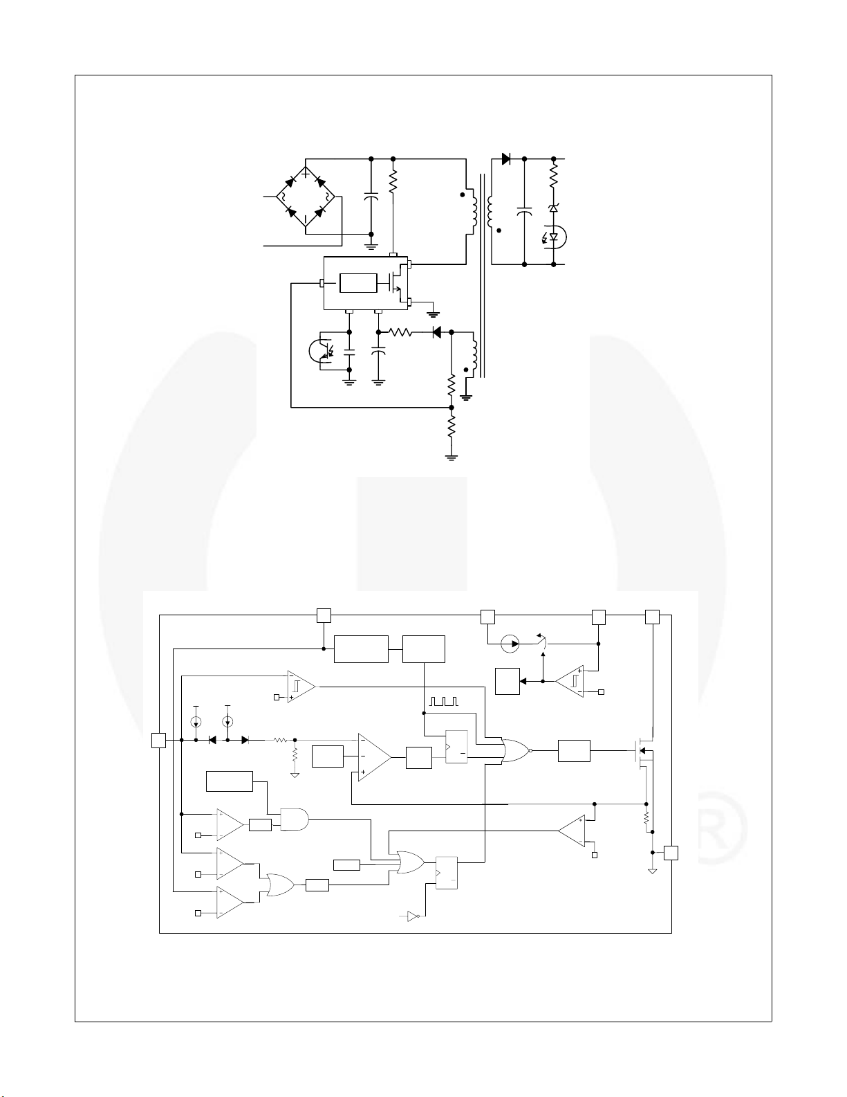
Figure 1. Typical Flyback Application
Sync
5
AVS
SoftStart
PWM
3R
R
OSC
LEB
250ns
FSQ0765R Rev.00
V
str
V
CC
Drain
3 16
V
ref
good
V
CC
Q
S
R
Q
Gate
driver
8V/12V
V
OSP
V
SD
V
OVP
LPF
LPF
TSD
VCC good
SQQ
R
AOCP
V
OCP
(1.1V)
FSQ0765R Rev.00
2
GND
Figure 2. Internal Block Diagram
© 2008 Fairchild Semiconductor Corporation www.fairchildsemi.com
FSQ0765RQ Rev. 1.0.1 3

Pin Configuration
6. V
5. Sync
4. FB
3. V
2. GND
1. Drain
FSQ0765R Rev.00
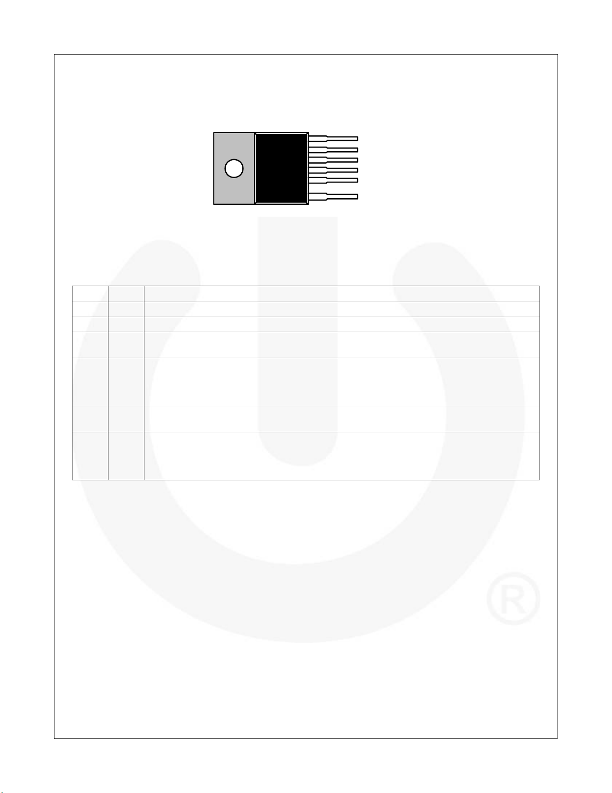
Figure 3. Pin Configuration (Top View)
Pin Definitions
Pin # Name Description
1DrainSenseFET drain. High-voltage power SenseFET drain connection.
2GNDGround. This pin is the control ground and the SenseFET source.
3V
4FB
5 Sync
6V
Power Supply. This pin is the positive supply input. This pin provides internal operating current for
CC
both startup and steady-state operation.
Feedback. This pin is internally connected to the inverting input of the PWM comparator. The
collector of an opto-coupler is typically tied to this pin. For stable operation, a capacitor should be
placed between this pin and GND. If the voltage of this pin reaches 6V, the overload protection
triggers, which shuts down the FPS.
Sync.
This pin is internally connected to the sync-detect comparator for quasi-resonant switching.
In normal quasi-resonant operation, the threshold of the sync comparator is 1.2V/1.0V.
Startup. This pin is connected directly, or through a resistor, to the high-voltage DC link. At
start-up, the internal high-voltage current source supplies internal bias and charges the external
str
capacitor connected to the VCC pin. Once VCC reaches 12V, the internal current source is disabled.
It is not recommended to connect V
and Drain together.
str
FSQ0765RQ — Green-Mode Farichild Power Switch (FPS™) for Quasi-Resonant Operation
str
CC
© 2008 Fairchild Semiconductor Corporation www.fairchildsemi.com
FSQ0765RQ Rev. 1.0.1 4

Absolute Maximum Ratings
Stresses exceeding the absolute maximum ratings may damage the device. The device may not function or be operable above the recommended operating conditions and stressing the parts to these levels is not recommended. In addition, extended exposure to stresses above the recommended operating conditions may affect device reliability. The
absolute maximum ratings are stress ratings only. T
Symbol Parameter Min. Max. Unit
V
str
V
DS
V
CC
V
FB
V
Sync
I
DM
I
D
E
AS
P
D
T
J
T
A
T
STG
ESD Electrostatic Discharge Capability
V
Pin Voltage 500 V
str
Drain Pin Voltage 650 V
Supply Voltage 20 V
Feedback Voltage Range -0.3 13.0 V
Sync Pin Voltage -0.3 13.0 V
Drain Current Pulsed 14.4 A
Continuous Drain Current
(6)
Single Pulsed Avalanche Energy
Total Power Dissipation(Tc=25°C) 45 W
Operating Junction Temperature Internally limited °C
Operating Ambient Temperature -25 +85 °C
Storage Temperature -55 +150 °C
= 25°C, unless otherwise specified.
A
TC = 25°C 3.6
T
= 100°C 2.28
(7)
C
Human Body Model 2
Charged Device Model 2
A
570 mJ
kV
FSQ0765RQ — Green-Mode Farichild Power Switch (FPS™) for Quasi-Resonant Operation
Notes:
6. Repetitive rating: Pulse width limited by maximum junction temperature.
7. L=81mH, starting TJ=25°C.
Thermal Impedance
TA = 25°C unless otherwise specified.
Symbol Parameter Value Unit
(9)
(8)
50
2.8
θ
JA
θ
JC
Junction-to-Ambient Thermal Resistance
Junction-to-Case Thermal Resistance
Notes:
8. Free standing with no heat-sink under natural convection.
9. Infinite cooling condition - refer to the SEMI G30-88.
°
C/W
°
C/W
© 2008 Fairchild Semiconductor Corporation www.fairchildsemi.com
FSQ0765RQ Rev. 1.0.1 5

FSQ0765RQ — Green-Mode Farichild Power Switch (FPS™) for Quasi-Resonant Operation
Electrical Characteristics
TA = 25°C unless otherwise specified.
Symbol Parameter Condition Min. Typ. Max. Unit
SENSEFET SECTION
BV
DSS
I
DSS
R
DS(ON)
C
OSS
t
d(on)
t
r
t
d(off)
t
f
CONTROL SECTION
t
ON.MAX
t
B
t
W
f
S
Δf
t
AVS
V
AVS
t
SW
I
FB
D
MIN
V
START
V
STOP
t
S/S
BURST-MODE SECTION
V
BURH
V
BURL
Hysteresis 200 mV
Drain Source Breakdown Voltage VCC = 0V, ID = 100µA 650 V
Zero-Gate-Voltage Drain Current VDS = 520V, VGS = 0V 300 µA
Drain-Source On-State Resistance TJ = 25°C, ID = 1.8A 1.3 1.6 Ω
Output Capacitance VGS = 0V, VDS = 25V, f = 1MHz 125 pF
Turn-On Delay Time
Rise Time 102 ns
Turn-Off Delay Time 63 ns
VDD = 325V, ID = 6.5A
27 ns
Fall Time 65 ns
Maximum On Time TJ = 25°C 8.8 10.0 11.2 µs
Blanking Time TJ = 25°C, V
Detection Time Window TJ = 25°C, V
= 5V 13.5 15.0 16.5 µs
sync
= 0V 6.0 µs
sync
Initial Switching Frequency 59.6 66.7 75.8 kHz
Switching Frequency Variation
S
AVS Triggering
Threshold
(11)
Switching Time Variance by AVS
(11)
On Time
Feedback
Voltage
(11)
-25°C < TJ < 85°C ±5 ±10 %
at V
= 240VDC, Lm = 360μH
IN
(AVS triggered when V
<spec.)
& t
AVS
AVS
Sync = 500kHz sine input
V
= 1.2V, t
FB
ON
= 4.0µs
>spec
13.5 20.5 µs
4.0 µs
1.2 V
Feedback Source Current VFB = 0V 700 900 1100 µA
Minimum Duty Cycle VFB = 0V 0 %
UVLO Threshold Voltage
After turn-on 7 8 9 V
11 12 13 V
Internal Soft-Start Time With free-running frequency 17.5 ms
0.45 0.55 0.65 V
Burst-Mode Voltages TJ = 25°C, tPD = 200ns
(10)
0.25 0.35 0.45 V
Note:
10. Propagation delay in the control IC.
Continued on the following page...
© 2008 Fairchild Semiconductor Corporation www.fairchildsemi.com
FSQ0765RQ Rev. 1.0.1 6
 Loading...