FSLV16211 — 24-Bit Bus Switch
FSLV16211 ⎯ 24-Bit Bus Switch
October 2010
Features
5Ω Switch Connection between Two Ports
Minimal Propagation Delay through the Switch
Low l
CC
Zero Bounce in Flow-Through Mode
Packaged in Thin-Shrink Small Outline Package
(TSSOP)
Ordering Information
Operating
Part Number
FSLV16211MTDX -40°C to 85°C
Temperature
Range
56-Lead, Thin Shrink Small Outline Package
(TSSOP), JEDEC M0-153, 6.1mm Wide
Description
The FSLV16211 is a 24-bit, high-speed, low-voltage
bus switch. The low on resistance of the switch allows
inputs to be connected to outputs without adding
propagation delay or generating additional ground
bounce noise.
This design can be used as a 12- or 24-bit bus switch.
When /OE1 is LOW, port 1A is connected to Port 1B.
When /OE2 is LOW, port 2A is connected to Port 2B.
Package Packing Method
Tape and Reel
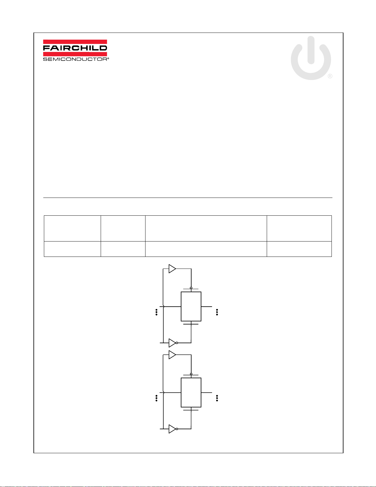
1A
1
1A
12
/OE
1
2A
1
2A
12
/OE
2
Figure 1. Logic Diagram
© 2003 Fairchild Semiconductor Corporation www.fairchildsemi.com
FSLV16211 Rev. 1.0.2
1B
1B
2B
2B
1
12
1
12

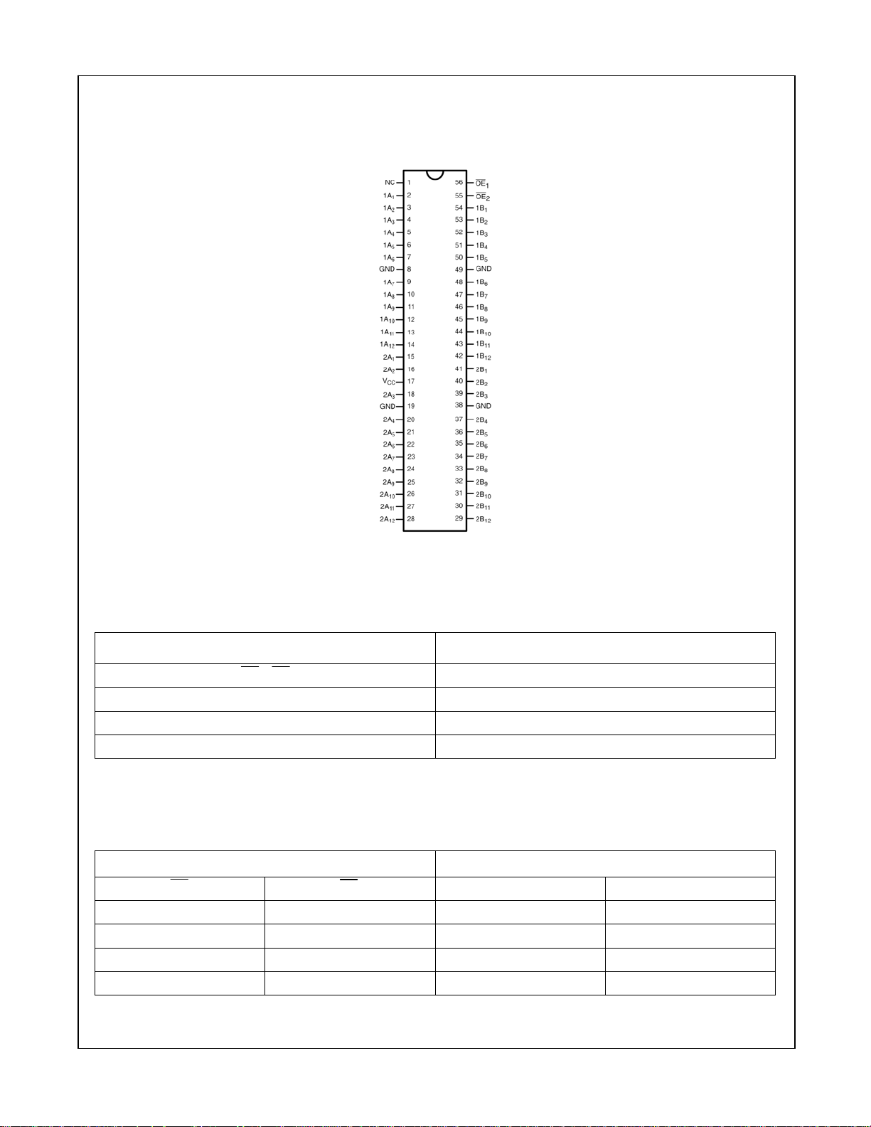
Connection Diagram
FSLV16211 ⎯ 24-Bit Bus Switch
Pin Description
Truth Table
OE1 OE2 1A,1B 2A, 2B
Low Low 1A=1B 2A=2B
Low High 1A=1B Z
High Low Z 2A=2B
High High Z Z
Figure 2. Pin Assignments for TSSOP
(Top Through View)
Pin Name Description
OE1, OE2 Bus Switch Enables
1A, 2A Bus A
1B, 2B Bus B
NC No Connect
Inputs Inputs/Outputs
© 2003 Fairchild Semiconductor Corporation www.fairchildsemi.com
FSLV16211 Rev. 1.0.2 2

FSLV16211⎯ 24-Bit Bus Switch
Absolute Maximum Ratings
Stresses exceeding the absolute maximum ratings may damage the device. The device may not function or be
operable above the recommended operating conditions and stressing the parts to these levels is not recommended.
In addition, extended exposure to stresses above the recommended operating conditions may affect device
reliability. The absolute maximum ratings are stress ratings only.
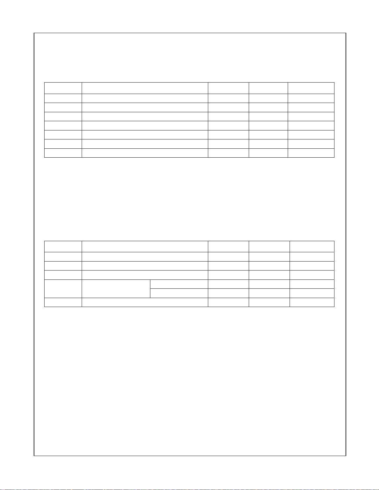
Symbol Parameter Min. Max. Unit
VCC Supply Voltage -0.5 4.6 V
VS DC Switch Voltage
VIN DC Input Voltage -0.5 4.6 V
IIK DC Input Diode Current -50 mA
I
DC Output Sink Current 128 mA
OUT
ICC/I
DC VCC/GND Current ±100 mA
GNG
T
Storage Temperature Range -65 150 °C
STG
Note:
1. The input and output negative voltage ratings may be exceeded if the input and output diode current ratings are
observed.
(1)
-0.5 4.6 V
Recommended Operating Conditions
The Recommended Operating Conditions table defines the conditions for actual device operation. Recommended
operating conditions are specified to ensure optimal performance to the datasheet specifications. Fairchild does not
recommend exceeding them or designing to Absolute Maximum Ratings.
Symbol Parameter Min. Max. Unit
VCC Power Supply Operating Voltage 2.3 3.6 V
VIN Input Voltage 0 3.6 V
V
Output Voltage 0 3.6 V
OUT
tr, tf Input Rise and Fall Time
TA Free Air Operating Temperature -40 85 °C
Note:
2. Unused control inputs must be held HIGH or LOW. They may not float.
Switch Control Input 0 4.0 ns/V
Switch I/O 0 DC ns/V
(2)
© 2003 Fairchild Semiconductor Corporation www.fairchildsemi.com
FSLV16211 Rev. 1.0.2 3
 Loading...