FSL137H
Green Mode Fairchild Power Switch (FPS™)
FSL137H — Green Mode Fairchild Power Switch (FPS™)
September 2010
Features
Built-in 5ms Soft-Start Function
Internal Avalanche Rugged 700V SenseFET
Low Audio Noise
High-Voltage Startup
Fixed PWM Frequency at 100KHz
Linearly Decreasing PWM Frequency to 18KHz
Peak-Current-Mode Control
Cycle-by-Cycle Current Limiting
Leading-Edge Blanking (LEB)
Synchronized Slope Compensation
Internal Open-loop Protection (OLP)
V
V
Under-Voltage Lockout (UVLO)
DD
Over-Voltage Protection (OVP)
DD
Constant Power Limit (Full AC Input Range)
Internal OTP Sensor with Hysteresis
Applications
General-purpose switch-mode power supplies and
flyback power converters, including:
SMPS for VCR, SVR, STB, DVD & VCD Player,
Printer, Facsimile, & Scanner
Adapter for Camcorder
Description
The highly integrated FSL137H consists of an
integrated current mode Pulse Width Modulator (PWM)
and an avalanche-rugged 700V SenseFET. It is
specifically designed for high-performance offline
Switch Mode Power Supplies (SMPS) with minimal
external components.
The integrated PWM controller features include a
proprietary green-mode function that provides off-time
modulation to linearly decrease the switching frequency
at light-load conditions to minimize standby power
consumption. To avoid acoustic noise problems, the
minimum PWM frequency is set above 18KHz. The
green-mode function enables the power supply to meet
international power conservation requirements. With the
internal high-voltage startup circuitry, the power loss
due to bleeding resistors is also eliminated. To further
reduce power consumption, the PWM controller is
manufactured using the BiCMOS process, which allows
an operating current of only 3.5mA.
The FSL137H built-in synchronized slope compensation
achieves stable peak-current-mode control. The
proprietary external line compensation ensures
constant output power limit over a wide AC input
voltage range, from 90V
The FSL137H provides many protection functions. In
addition to cycle-by-cycle current limiting, the internal
open-loop protection circuit ensures safety when an
open-loop or output short-circuit failure occurs. PWM
output is disabled until V
limit, when the controller starts up again. As long as V
exceeds ~28V, the internal OVP circuit is triggered.
Compared to a discrete MOSFET and controller or RCC
switching converter solution, the FSL137H reduces total
component count, design size, and weight while
increasing efficiency, productivity, and system reliability.
These devices provide a basic platform well suited for
design of cost-effective flyback converters.
to 264VAC.
AC
drops below the UVLO lower
DD
DD
Ordering Information
Part Number SenseFET
FSL137HNY 3.0A 700V -40°C to +105°C 8-Pin Dual In-Line Package (DIP) Tube
© 2009 Fairchild Semiconductor Corporation www.fairchildsemi.com
FSL137H Rev. 1.0.3
Operating Temperature
Range
Package
Packing
Method

Application Diagram
HV
Drain
VIN
GNDVDDFB
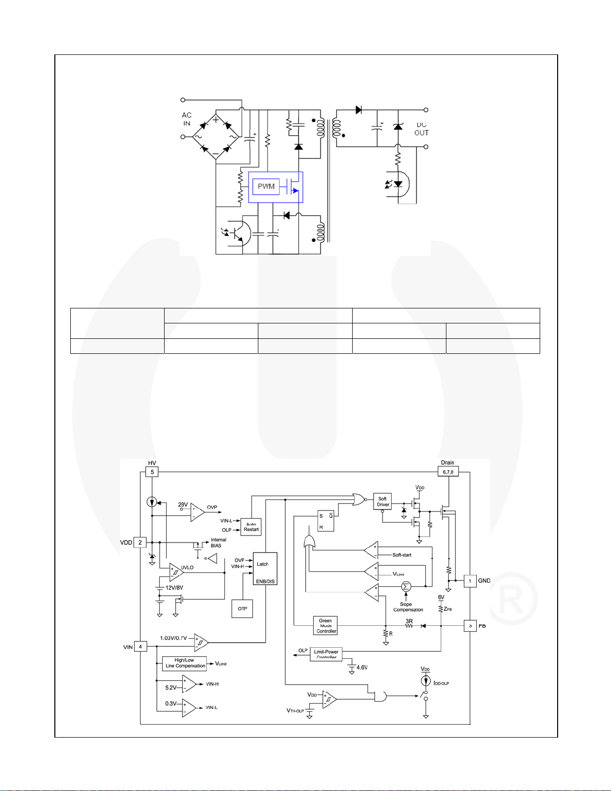
Figure 1. Typical Flyback Application
FSL137H — Green Mode Fairchild Power Switch (FPS™)
Output Power Table
Product
(1)
Adapter
(2)
± 15%
230V
AC
(3)
Open Frame
85-265VAC
(4)
Adapter
(3)
Open Frame
FSL137H 17.5W 25W 13W 19W
Notes:
1. The maximum output power can be limited by junction temperature.
2. 230 V
or 100/115 V
AC
with doublers.
AC
3. Typical continuous power in a non-ventilated enclosed adapter with sufficient drain pattern as a heat sink,
at T
=50°C ambient.
A
4. Maximum practical continuous power in an open-frame design with sufficient drain pattern as a heat sink,
at T
=50°C ambient.
A
Internal Block Diagram
(4)
Figure 2. Internal Block Diagram
© 2009 Fairchild Semiconductor Corporation www.fairchildsemi.com
FSL137H Rev. 1.0.3

Pin Configuration
FSL137H — Green Mode Fairchild Power Switch (FPS™)
Pin Definitions
Pin # Name Description
1 GND
2 VDD
3 FB
4 VIN
5 HV
6 Drain
7 Drain
8 Drain
Ground. SenseFET source terminal on primary side and internal controller ground.
Power Supply. The internal protection circuit disables PWM output as long as V
OVP trigger point.
Feedback. The signal from the external compensation circuit is fed into this pin. The PWM duty
cycle is determined in response to the signal on this pin and the internal current-sense signal.
Line-Voltage Detection. The line-voltage detection is used for brownout protection with
hysteresis and constant output power limit over universal AC input range. This pin has additional
protections that are pull-HIGH latch and pull-low auto recovery, depending on the application.
Startup. For startup, this pin is pulled HIGH to the line input or bulk capacitor via resistors.
SenseFET Drain. High-voltage power SenseFET drain connection.
SenseFET Drain. High-voltage power SenseFET drain connection.
SenseFET Drain. High-voltage power SenseFET drain connection.
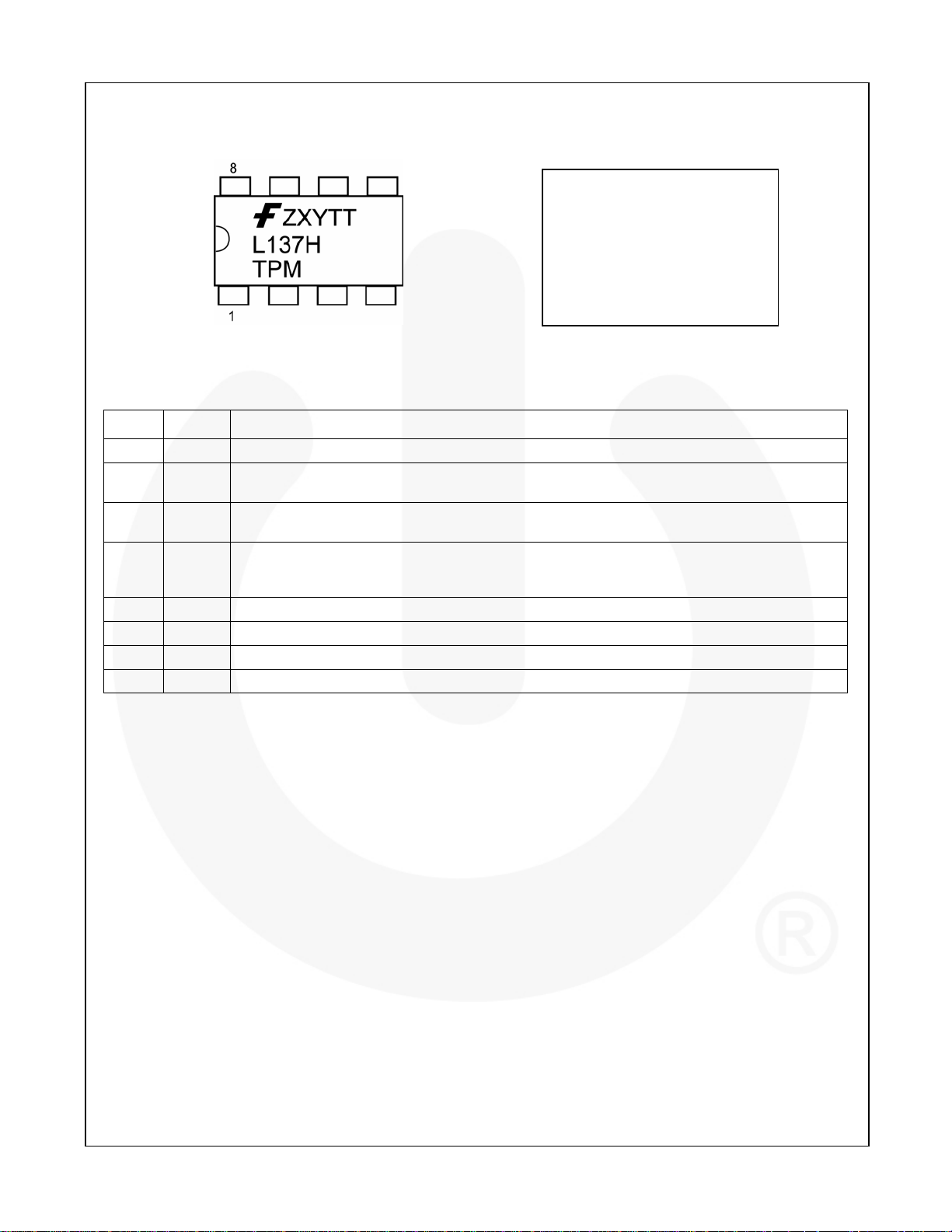
F – Fairchild Logo
Z – Plant Code
X – 1-Digit Year Code
Y – 1-Digit Week Code
TT – 2-Digit Die Run Code
T – Package Type (N: DIP)
P – Y: Green Package
M – Manufacture Flow Code
Figure 3. Pin Configuration
exceeds the
DD
© 2009 Fairchild Semiconductor Corporation www.fairchildsemi.com
FSL137H Rev. 1.0.3 3

FSL137H — Green Mode Fairchild Power Switch (FPS™)
Absolute Maximum Ratings
Stresses exceeding the absolute maximum ratings may damage the device. The device may not function or be
operable above the recommended operating conditions and stressing the parts to these levels is not recommended.
In addition, extended exposure to stresses above the recommended operating conditions may affect device
reliability. The absolute maximum ratings are stress ratings only.
Symbol Parameter Min. Max. Unit
V
Drain Pin Voltage
DRAIN
IDM Drain Current Pulsed
EAS Single Pulsed Avalanche Energy
V
DC Supply Voltage 30 V
VDD
VFB FB Pin Input Voltage -0.3 7.0 V
V
VIN Pin Input Voltage -0.3 7.0 V
VIN
VHV HV Pin Input Voltage 700 V
Power Dissipation (T
PD
θJA Junction-to-Air Thermal Resistance
ΨJT Junction-to-Top Thermal Resistance
TJ Operating Junction Temperature
T
Storage Temperature Range
STG
TL Lead Temperature (Wave Soldering or IR, 10 Seconds)
ESD
Electrostatic Discharge Capability,
All Pins Except HV Pin
Notes:
5. All voltage values, except differential voltages, are given with respect to the network ground terminal.
6. Stresses beyond those listed under Absolute Maximum Ratings may cause permanent damage to the device.
7. Non-repetitive rating: Pulse width is limited by maximum junction temperature.
8. L = 51mH, starting T
9. Measured on the package top surface.
10. All pins including HV pin: HBM=1kV, CDM=1.25kV
(5, 6)
700 V
(7)
12 A
(8)
230 mJ
A
= 25°C.
J
<50°C)
(10)
(9)
Human Body Model: JESD22-A114 4.5
Charged Device Model: JESD22-C101 1.5
-55
1.5 W
80
35
+150
150
+260
°C/W
°C/W
°C
°C
°C
kV
Recommended Operating Conditions
The Recommended Operating Conditions table defines the conditions for actual device operation. Recommended
operating conditions are specified to ensure optimal performance to the datasheet specifications. Fairchild does not
recommend exceeding them or designing to Absolute Maximum Ratings.
Symbol Parameter Conditions Min. Typ. Max. Unit
TA Operating Ambient Temperature -40 +105 °C
© 2009 Fairchild Semiconductor Corporation www.fairchildsemi.com
FSL137H Rev. 1.0.3 4

FSL137H — Green Mode Fairchild Power Switch (FPS™)
Electrical Characteristics
VDD=15V, TA=25°C unless otherwise specified.
Symbol Parameter Conditions Min. Typ. Max. Unit
SenseFET Section
BV
Drain-Source Breakdown Voltage VGS = 0V 700 V
DSS
I
Zero-Gate-Voltage Drain Current
DSS
R
Drain-Source On-State Resistance
DS(ON)
C
Input Capacitance
ISS
C
Output Capacitance
OSS
C
Reverse Transfer Capacitance
RSS
t
Turn-On Delay Time VDS = 350V, ID = 1.0A 11.2 33.0 ns
d(on)
tr Rise Time VDS = 350V, ID = 1.0A 34 78 ns
t
Turn-Off Delay Time VDS = 350V, ID = 1.0A 28.2 67.0 ns
d(off)
tf Fall Time VDS = 350V, ID = 1.0A 32 74 ns
VDD Section
VOP Continuously Operating Voltage 22 V
V
Start Threshold Voltage 11 12 13 V
DD-ON
V
Minimum Operating Voltage 7 8 9 V
DD-OFF
I
Startup Current V
DD-ST
I
Operating Supply Current VDD = 15V, VFB = 3V 3.0 3.5 4.0 mA
DD-OP
I
DD-BM
I
Internal Sink Current
DD-OLP
V
I
TH-OLP
V
VDD Over-Voltage Protection 27 28 29 V
DD-OVP
t
D-VDDOVP
HV Section
IHV Maximum Current Drawn from HV Pin
I
Leakage Current After Startup
HV-LC
Oscillator Section
f
Frequency in Nominal Mode
OSC
f
Green-Mode Frequency 14 18 22 kHz
OSC-G
D
Maximum Duty Cycle 85 %
MAX
fDV Frequency Variation vs. VDD Deviation VDD = 9V to 22V 5 %
fDT
(11)
VDS = 700V, VGS = 0V 0.5 50.0
VDS = 560V, VGS = 0V,
T
= 125°C
A
(12)
VGS = 10V, ID = 0.5A 4.00 4.75 Ω
VGS = 0V, VDS = 25V,
f = 1MHz
= 0V, VDS = 25V,
V
GS
f = 1MHz
VGS = 0V, VDS = 25V,
f = 1MHz
– 0.16V 30 µA
DD-ON
Green-Mode Operating Supply
Current
Off Voltage 5 6 7 V
DD-OLP
Over-Voltage Protection
V
DD
Debounce Time
VFB = V
V
TH-OLP
2 mA
FB-G
+0.1V
75 130 200 µs
HV 120V
V
= 0V with 10µF
DD
DC
,
HV = 700V,
V
DD
= V
DD-OFF
+1V
Center Frequency
Frequency Variation vs. Temperature
Deviation
(11)
= -40 to +105°C
T
A
1 200
315 410 pF
47 61 pF
9 14 pF
30 60 90 µA
1.5 3.5 5.0 mA
1 20
94 100 106 kHz
5 %
μA
µA
Continued on the following page…
© 2009 Fairchild Semiconductor Corporation www.fairchildsemi.com
FSL137H Rev. 1.0.3 5
 Loading...