

Fairchild FSL136MRT service manual
FSL136MRT
Green-Mode Fairchild Power Switch (FPS™)
FSL136MRT — Green-Mode Fairchild Power Switch (FPS™)
May 2012
Features
Internal Avalanched-Rugged 650V SenseFET
Advanced Soft Burst-Mode Operation for Low
Standby Power and Low Audible Noise
Random Frequency Fluctuation for Low EMI
Pulse-by-Pulse Current Limit
Various Protection Functions: Overload Protection
(OLP), Over-Voltage Protection (OVP), Abnormal
Over-Current Protection (AOCP), Internal Thermal
Shutdown (TSD) with Hysteresis, and Under-Voltage
Lockout (UVLO) with Hysteresis
Low Operating Current (0.4mA) in Burst Mode
Internal Startup Circuit
Built-in Soft-Start: 15ms
Auto-Restart Mode
Applications
Power Supply for STB Home Appliances and
DVD Combination
Description
The FSL136MRT is an integrated Pulse Width
Modulation (PWM) controller and SenseFET specifically
designed for offline Switch-Mode Power Supplies
(SMPS) with minimal external components. The PWM
controller includes an integrated fixed-frequency
oscillator, Under-Voltage Lockout (UVLO), LeadingEdge Blanking (LEB), optimized gate driver, internal
soft-start, temperature-compensated precise current
sources for loop compensation, and self-protection
circuitry. Compared with a discrete MOSFET and PWM
controller solution, the FSL136MRT can reduce total
cost, component count, size, and weight; while
simultaneously increasing efficiency, productivity, and
system reliability. This device provides a basic platform
suited for cost-effective design of a flyback converter.
Ordering Information
(2)
(4)
Open
Frame
Replaces
Device
(5)
KA5M0365RY
DTU
Operating
Part Number Package
TO-220F
FSL136MRT
Notes:
1. Pb-free package per JEDEC J-STD-020B.
2. The junction temperature can limit the maximum output power.
3. 230V
4. Typical continuous power in a non-ventilated enclosed adapter measured at 50°C ambient temperature.
5. Maximum practical continuous power in an open-frame design at 50°C ambient temperature.
© 2012 Fairchild Semiconductor Corporation www.fairchildsemi.com
FSL136MRT • Rev. 1.0.0
6-Lead
W-Forming
or 100/115VAC with voltage doubler.
AC
Temperature
(1)
Junction
-40°C ~
+125°C
Current
Limit
2.15A
R
DS(ON)
(Max.)
4Ω
Adapter
Output Power Table
230VAC ± 15%
(4)
35W 50W 24W 35W
(3)
85~265VAC
Open
Frame
Adapter
(5)
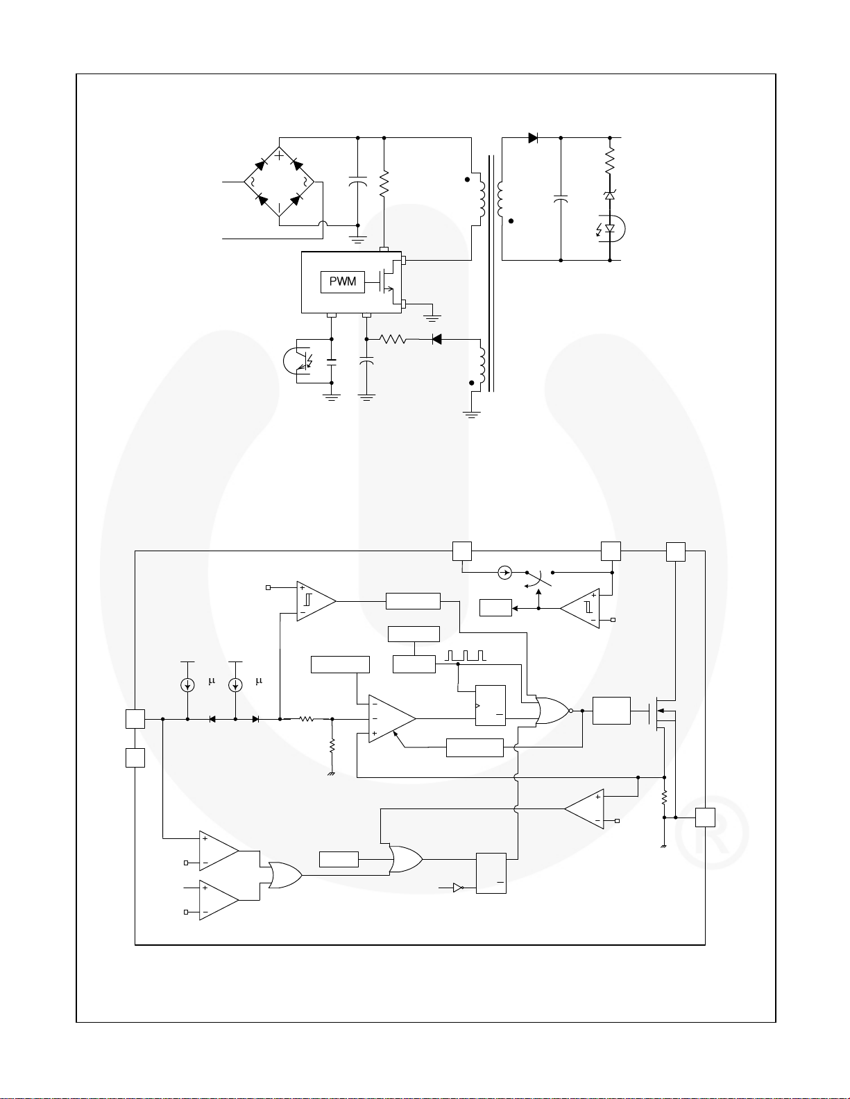
Application Circuit
AC
IN
FSL136MRT — Green-Mode Fairchild Power Switch (FPS™)
V
O
V
STR
Drain
GND
Internal Block Diagram
V
BURST
0.30V / 0.45V
FB
NC 5
V
4
CC
2.0 A
I
DELAY
V
REF
90 A
I
FB
FB
V
CC
Figure 1. Typical Application Circuit
V
STR
6 3
I
CH
3R
Soft-Start
R
Soft Burst
Random
OSC
PWM
V
SQ
R
LEB (350ns)
REF
Q
VCCGood
V
CC
Gate
Driver
Drain
1
7.5V / 12V
2
GND
V
SD
7.0V
V
CC
V
OVP
24.5V
TSD
VCCGood
SQ
R
Q
V
AOCP
Figure 2. Internal Block Diagram
© 2012 Fairchild Semiconductor Corporation www.fairchildsemi.com
FSL136MRT • Rev. 1.0.0 2
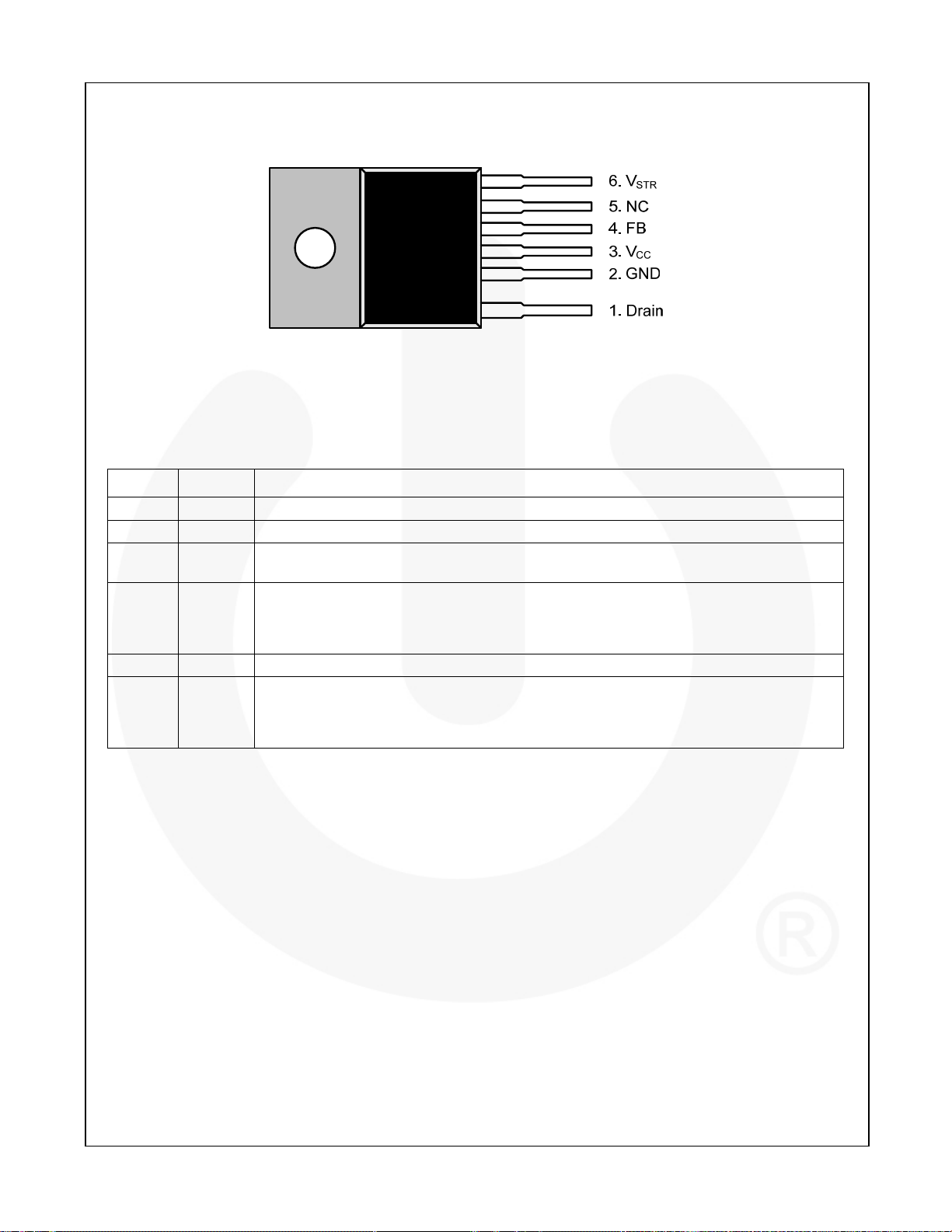
Pin Configuration
Figure 3. Pin Configuration (Top View)
Pin Definitions
Pin # Name Description
1 Drain
2 GND
3 VCC
4 FB
5 NC No Connection
6 V
STR
SenseFET Drain. High-voltage power SenseFET drain connection.
Ground. This pin is the control ground and the SenseFET source.
Power Supply. This pin is the positive supply input, which provides the internal operating
current for both startup and steady-state operation.
Feedback. This pin is internally connected to the inverting input of the PWM comparator.
The collector of an opto-coupler is typically tied to this pin. For stable operation, a capacitor
should be placed between this pin and GND. If the voltage of this pin reaches 7V, the
overload protection triggers, which shuts down the FPS.
Startup. This pin is connected directly, or through a resistor, to the high-voltage DC link.
At startup, the internal high-voltage current source supplies internal bias and charges the
external capacitor connected to the V
source (I
) is disabled.
CH
pin. Once VCC reaches 12V, the internal current
CC
FSL136MRT — Green-Mode Fairchild Power Switch (FPS™)
© 2012 Fairchild Semiconductor Corporation www.fairchildsemi.com
FSL136MRT • Rev. 1.0.0 3
FSL136MRT — Green-Mode Fairchild Power Switch (FPS™)
Absolute Maximum Ratings
Stresses exceeding the absolute maximum ratings may damage the device. The device may not function or be
operable above the recommended operating conditions and stressing the parts to these levels is not recommended.
In addition, extended exposure to stresses above the recommended operating conditions may affect device reliability.
The absolute maximum ratings are stress ratings only.
Symbol Parameter Min. Max. Unit
V
V
STR
V
Drain Pin Voltage 650 V
DS
V
V
CC
V
Feedback Pin Voltage -0.3 10.0 V
FB
I
Drain Current Pulsed
DM
IDS Continuous Switching Drain Current 3 A
E
Single Pulsed Avalanche Energy
AS
PD Total Power Dissipation (TC=25°C)
T
J
T
Storage Temperature -55 +150
STG
Notes:
6. Repetitive peak switching current when the inductive load is assumed: Limited by maximum duty (D
and junction temperature (see Figure 4).
7. L=45mH, starting T
8. Infinite cooling condition (refer to the SEMI G30-88).
9. Although this parameter guarantees IC operation, it does not guarantee all electrical characteristics.
Pin Voltage 650 V
STR
Pin Voltage 26 V
CC
(6)
12 A
(7)
230 mJ
(8)
50 W
Maximum Junction Temperature 150
Operating Junction Temperature
=25°C.
J
(9)
-40 +125
MAX
°C
°C
°C
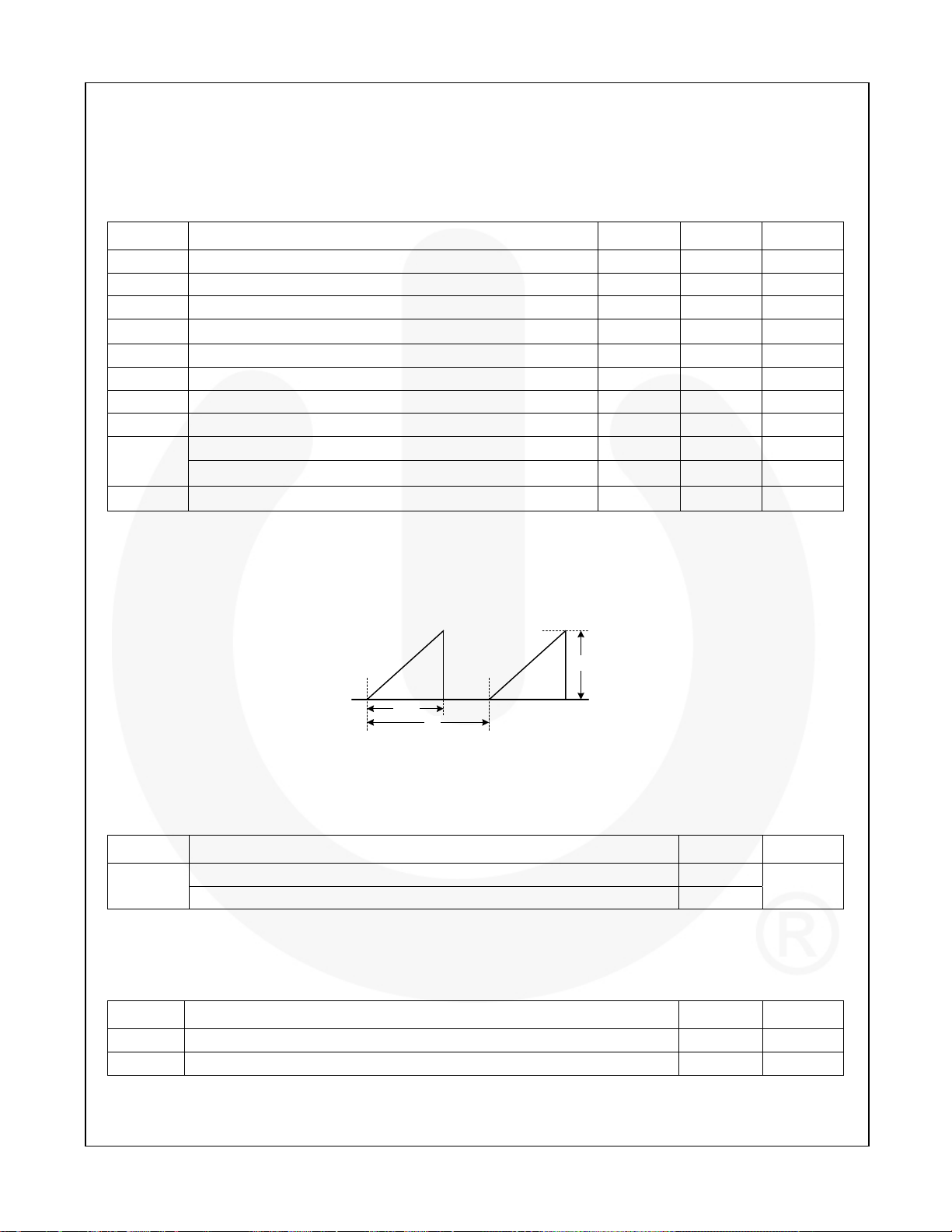
=0.74)
I
DS
D
MAX
f
SW
Figure 4. Repetitive Peak Switching Current
ESD Capability
Symbol Parameter Value Unit
ESD
Human Body Model, JESD22-A114 5
Charged Device Model, JESD22-C101 2
KV
Thermal Impedance
TA=25°C unless otherwise specified.
Symbol Parameter Value Unit
JA Junction-to-Ambient Thermal Impedance
JC Junction-to-Case Thermal Impedance
Notes:
10. Free standing without heat sink under natural convection condition, per JEDEC 51-2 and 1-10.
11. Infinite cooling condition per Mil Std. 883C method 1012.1.
(10)
63.5 °C/W
(11)
2.8 °C/W
© 2012 Fairchild Semiconductor Corporation www.fairchildsemi.com
FSL136MRT • Rev. 1.0.0 4
 Loading...