

Fairchild FSL116HR service manual
FSL116HR
Green Mode Fairchild Power Switch (FPS™)
FSL116HR — Green Mode Fairchild Power Switch (FPS™)
April 2012
Features
Internal Avalanche-Rugged SenseFET (650V)
Under 50mW Standby Power Consumption at
265V
, No-load Condition with Burst Mode
AC
Precision Fixed Operating Frequency with
Frequency Modulation for Attenuating EMI
Internal Startup Circuit
Built-in Soft-Start: 20ms
Pulse-by-Pulse Current Limiting
Various Protections: Over-Voltage Protection
(OVP), Overload Protection (OLP), Output-Short
Protection (OSP), Abnormal Over-Current
Protection (AOCP), Internal Thermal Shutdown
Function with Hysteresis (TSD)
Auto-Restart Mode
Under-Voltage Lockout (UVLO)
Low Operating Current: 1.8mA
Adjustable Peak Current Limit
Applications
SMPS for VCR, STB, DVD, & DVCD Players
SMPS for Home Appliance
Adapter
Related Resources
AN-4137 — Design Guidelines for Offline Flyback
Converters Using FPS™
AN-4141 — Troubleshooting and Design Tips for
Fairchild Power Switch (FPS™) Flyback
Applications
AN-4147 — Design Guidelines for RCD Snubber of
Flyback
Fairchild Power Supply WebDesigner — Flyback
Design & Simulation - In Minutes at No Expense
Description
The FSL116HR integrated Pulse Width Modulator
(PWM) and SenseFET is specifically designed for highperformance offline Switched-Mode Power Supplies
(SMPS) with minimal external components. FSL116HR
includes integrated high-voltage power switching
regulators that combine an avalanche-rugged
SenseFET with a Current-Mode PWM control block.
The integrated PWM controller includes: Under-Voltage
Lockout (UVLO) protection, Leading-Edge Blanking
(LEB), a frequency generator for EMI attenuation, an
optimized gate turn-on / turn-off driver, Thermal
Shutdown (TSD) protection, and temperaturecompensated precision current sources for loop
compensation and fault-protection circuitry. The
FSL116HR offers good soft-start performance. When
compared to a discrete MOSFET and controller or RCC
switching converter solution, the FSL116HR reduces
total component count, design size, and weight; while
increasing efficiency, productivity, and system reliability.
This device provides a basic platform that is well suited
for the design of cost-effective flyback converters.
Maximum Output Power
230VAC ±15%
Adapter
Notes:
1. The junction temperature can limit the maximum
2. 230V
3. Typical continuous power in a non-ventilated
(3)
11W 16W 10W 14W
output power.
or 100/115VAC with doubler.
AC
enclosed adapter measured at 50°C ambient.
(2)
85-265VAC
Open
Frame
Adapter
(1)
(3)
Open
Frame
Ordering Information
Part Number
FSL116HR -40 to 105°C FSL116HR 8-Lead, Dual Inline Package (DIP) Rail
© 2010 Fairchild Semiconductor Corporation www.fairchildsemi.com
FSL116HR • Rev. 1.0.1
Operating
Temperature Range
Top Mark Package Packing Method
D
n
V
V
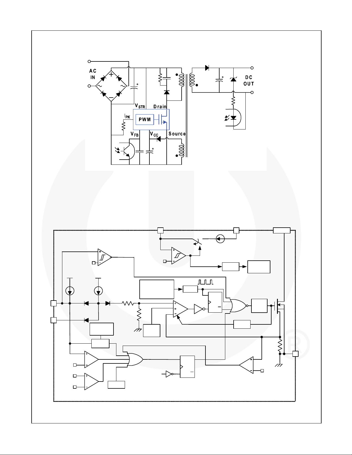
Typical Application Diagram
FSL116HR — Green Mode Fairchild Power Switch (FPS™)
Figure 1. Typical Application
Internal Block Diagram
V
BURL/VBURH
DELAY
V
CC
I
FB
On-Tim e
Detector
OSP
TSD
V
CC
I
3
FB
I
4
PK
V
SD
V
CC
V
OVP
2.5R
8V/12V
Freque ncy
Generator
R
Start
VCCGood
V
CC
2 6,7,8
VCCGood
STR
5
I
CH
V
REF
Intern al
Bias
Random
OSC
SQQ
Soft
PWM
S
R
Q
Gate
Driver
LEB
AOCP
R
Q
V
AOCP
rai
1
GND
Figure 2. Internal Block Diagram
© 2010 Fairchild Semiconductor Corporation www.fairchildsemi.com
FSL116HR • Rev. 1.0.1 2
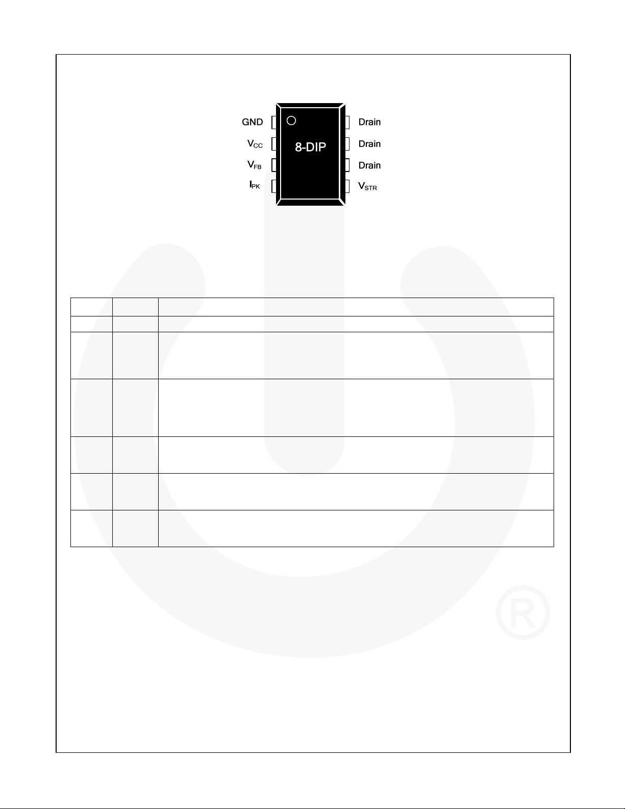
Pin Configuration
Figure 3. Pin Configuration
Pin Definitions
Pin # Name Description
1 GND
2 VCC
3 VFB
4 IPK
5 V
6, 7, 8 Drain
Ground. SenseFET source terminal on the primary side and internal control ground.
Positive Supply Voltage Input. Although connected to an auxiliary transformer winding,
current is supplied from pin 5 (V
V
reaches the UVLO upper threshold (12V), the internal startup switch opens and device
CC
) via an internal switch during startup (see Figure 2). Once
STR
power is supplied via the auxiliary transformer winding.
Feedback Voltage. The non-inverting input to the PWM comparator, it has a 0.4mA current
source connected internally, while a capacitor and opto-coupler are typically connected
externally. There is a delay while charging external capacitor CFB from 2.4V to 6V using an
internal 5µA current source. This delay prevents false triggering under transient conditions, but
still allows the protection mechanism to operate under true overload conditions.
Peak Current Limit. Adjusts the peak current limit of the SenseFET. The feedback 0.4mA
current source is diverted to the parallel combination of an internal 6k resistor and any
external resistor to GND on this pin to determine the peak current limit.
Startup. Connected to the rectified AC line voltage source. At startup, the internal switch
supplies internal bias and charges an external storage capacitor placed between the VCC pin
STR
and ground. Once V
reaches 12V, the internal switch is opened.
CC
Drain. Designed to connect directly to the primary lead of the transformer and capable of
switching a maximum of 650V. Minimizing the length of the trace connecting these pins to the
transformer decreases leakage inductance.
FSL116HR — Green Mode Fairchild Power Switch (FPS™)
© 2010 Fairchild Semiconductor Corporation www.fairchildsemi.com
FSL116HR • Rev. 1.0.1 3
FSL116HR — Green Mode Fairchild Power Switch (FPS™)
Absolute Maximum Ratings
Stresses exceeding the absolute maximum ratings may damage the device. The device may not function or be
operable above the recommended operating conditions and stressing the parts to these levels is not recommended.
In addition, extended exposure to stresses above the recommended operating conditions may affect device reliability.
The absolute maximum ratings are stress ratings only. T
Symbol Parameter Min. Max. Unit
V
V
STR
VDS Drain Pin Voltage -0.3 650.0 V
VCC Supply Voltage 26 V
VFB Feedback Voltage Range -0.3 12 V
ID Continuous Drain Current 1 A
IDM Drain Current Pulsed
EAS Single Pulsed Avalanche Energy
PD Total Power Dissipation 1.5 W
TJ Operating Junction Temperature Internally Limited °C
TA Operating Ambient Temperature -40 +105 °C
T
Storage Temperature -55 +150 °C
STG
ESD
ΘJA
ΘJC
ΘJT
Notes:
4. Repetitive rating: pulse width limited by maximum junction temperature.
5. L=30mH, starting T
6. Meets JEDEC standards JESD 22-A114 and JESD 22-C101.
7. All items are tested with the standards JESD 51-2 and JESD 51-10.
8. Θ
9. Θ
free-standing, with no heat-sink, under natural convection.
JA
junction-to-lead thermal characteristics under ΘJA test condition. TC is measured on the source #7 pin closed
JC
to plastic interface for Θ
10. Θ
junction-to-top of thermal characteristic under ΘJA test condition. Tt is measured on top of package. Thermo-
JT
couple is mounted in epoxy glue.
Pin Voltage -0.3 650.0 V
STR
(4)
4 A
(5)
Human Body Model, JESD22-A114
Charged Device Model, JESD22-C101
Junction-to-Ambient Thermal Resistance
Junction-to-Case Thermal Resistance
Junction-to-Top Thermal Resistance
=25°C.
J
thermo-couple mounted on soldering.
JA
= 25°C, unless otherwise specified.
J
38 mJ
(6)
5
(6)
2
(7,8)
80 °C/W
(7,9)
19 °C/W
(7,10)
33.7 °C/W
KV
© 2010 Fairchild Semiconductor Corporation www.fairchildsemi.com
FSL116HR • Rev. 1.0.1 4
 Loading...