

Fairchild FSGM0565R service manual

FSGM0565R — Green-Mode Fairchild Power Switch (FPS™)
FSGM0565R
Green-Mode Fairchild Power Switch (FPS™)
Features
Soft Burst-Mode Operation for Low Standby Power
Consumption and Low Noise
Precision Fixed Operating Frequency: 66kHz
Pulse-by-Pulse Current Limit
Various Protection Functions: Overload Protection
(OLP), Over-Voltage Protection (OVP), Abnormal
Over-Current Protection (AOCP), Internal Thermal
Shutdown (TSD) with Hysteresis, Output Short
Protection (OSP), and Under-Voltage Lockout
(UVLO) with Hysteresis
Auto-Restart Mode
Internal Startup Circuit
Internal High-Voltage SenseFET: 650V
Built-in Soft-Start: 15ms
Description
The FSGM0565R is an integrated Pulse Width
Modulation (PWM) controller and SenseFET specifically
designed for offline Switch-Mode Power Supplies
(SMPS) with minimal external components. The PWM
controller includes an integrated fixed-frequency
oscillator, Under-Voltage Lockout (UVLO), LeadingEdge Blanking (LEB), optimized gate driver, internal
soft-start, temperature-compensated precise current
sources for loop compensation, and self-protection
circuitry. Compared with a discrete MOSFET and PWM
controller solution, the FSGM series can reduce total
cost, component count, size, and weight; while
simultaneously increasing efficiency, productivity, and
system reliability. This device provides a basic platform
suited for cost-effective design of a flyback converter.
March 2010
Applications
Power Supply for LCD TV and Monitor, STB and DVD
Combination
Ordering Information
(2)
(4)
Open
Frame
(5)
Replaces
Device
Part Number Package
FSGM0565RWDTU
FSGM0565RUDTU
FSGM0565RLDTU
Notes:
1. Pb-free package per JEDEC J-STD-020B.
2. The junction temperature can limit the maximum output power.
3. 230V
4. Typical continuous power in a non-ventilated enclosed adapter measured at 50°C ambient temperature.
5. Maximum practical continuous power in an open-frame design at 50°C ambient temperature.
or 100/115VAC with voltage doubler.
AC
TO-220F
6-Lead(1)
W-Forming
TO-220F
6-Lead(1)
U-Forming
TO-220F
6-Lead(1)
L-Forming
Operating
Junction
Temperature
-40°C ~
+125°C
-40°C ~
+125°C
-40°C ~
+125°C
Current
Limit
2.20A
2.20A
2.20A
R
DS(ON)
(Max.)
2.2Ω
2.2Ω
2.2Ω
Adapter
Output Power Table
(4)
(3)
85~265VAC
Open
Frame
Adapter
(5)
230VAC ± 15%
70W 80W 41W 60W FSDM0565RE
70W 80W 41W 60W FSDM0565RE
70W 80W 41W 60W FSDM0565RE
© 2009 Fairchild Semiconductor Corporation www.fairchildsemi.com
FSGM0565R • Rev. 1.0.2
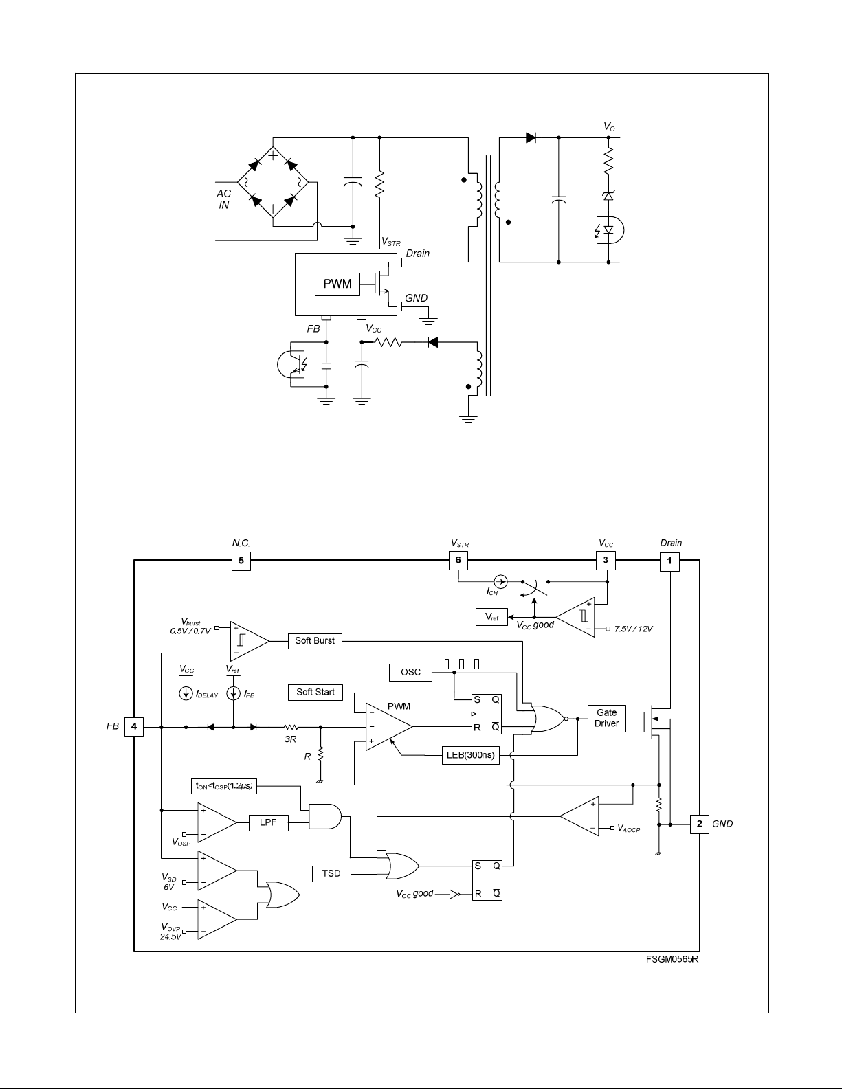
Application Circuit
FSGM0565R — Green-Mode Fairchild Power Switch (FPS™)
Internal Block Diagram
Figure 1. Typical Application Circuit
Figure 2. Internal Block Diagram
© 2009 Fairchild Semiconductor Corporation www.fairchildsemi.com
FSGM0565R • Rev. 1.0.2 2
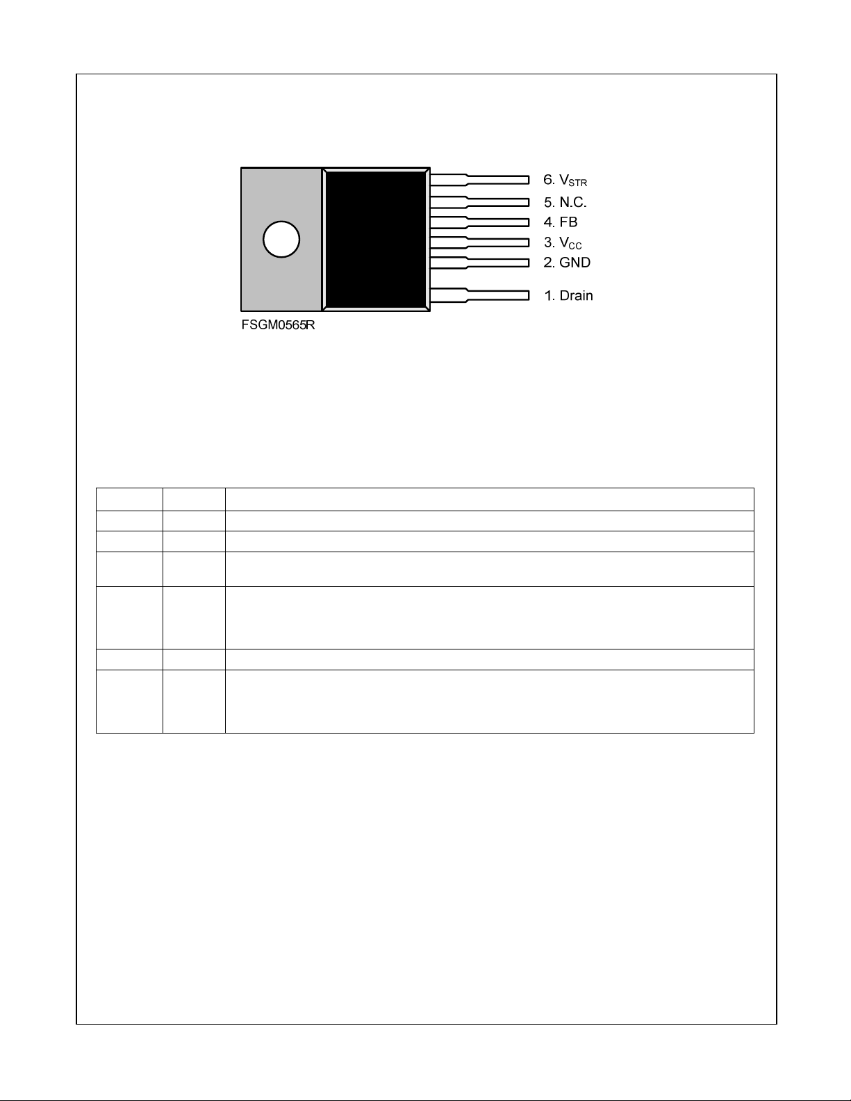
Pin Configuration
FSGM0565R — Green-Mode Fairchild Power Switch (FPS™)
Figure 3. Pin Configuration (Top View)
Pin Definitions
Pin # Name Description
1 Drain SenseFET Drain. High-voltage power SenseFET drain connection.
2 GND Ground. This pin is the control ground and the SenseFET source.
3 VCC
4 FB
5 N.C. No connection.
6 V
Power Supply. This pin is the positive supply input, which provides the internal operating
current for both startup and steady-state operation.
Feedback. This pin is internally connected to the inverting input of the PWM comparator. The
collector of an opto-coupler is typically tied to this pin. For stable operation, a capacitor
should be placed between this pin and GND. If the voltage of this pin reaches 6V, the
overload protection triggers, which shuts down the FPS.
Startup. This pin is connected directly, or through a resistor, to the high-voltage DC link. At
startup, the internal high-voltage current source supplies internal bias and charges the
STR
external capacitor connected to the V
source (I
) is disabled.
CH
pin. Once VCC reaches 12V, the internal current
CC
© 2009 Fairchild Semiconductor Corporation www.fairchildsemi.com
FSGM0565R • Rev. 1.0.2 3

FSGM0565R — Green-Mode Fairchild Power Switch (FPS™)
Absolute Maximum Ratings
Stresses exceeding the absolute maximum ratings may damage the device. The device may not function or be
operable above the recommended operating conditions and stressing the parts to these levels is not recommended.
In addition, extended exposure to stresses above the recommended operating conditions may affect device
reliability. The absolute maximum ratings are stress ratings only.
Symbol Parameter Min. Max. Unit
V
V
STR
VDS Drain Pin Voltage 650 V
VCC VCC Pin Voltage 26 V
VFB Feedback Pin Voltage -0.3 12 V
IDM Drain Current Pulsed 11 A
IDS Continuous Switching Drain Current
EAS Single Pulsed Avalanche Energy
PD
TJ
T
STG
V
Minimum Isolation Range
ISO
ESD
Notes:
6. Repetitive peak switching current when the inductive load is assumed: Limited by maximum duty (D
and junction temperature (see Figure 4).
7. L=45mH, starting TJ=25°C.
8. Infinite cooling condition (refer to the SEMI G30-88).
9. Although this parameter guarantees IC operation, it does not guarantee all electrical characteristics.
10. The voltage between the package back side and the lead is guaranteed.
Pin Voltage 650 V
STR
5.6 A
3.4 A
45 W
+150
-40 +125
-55 +150
°C
°C
°C
kV
=0.75)
MAX
Total Power Dissipation (TC=25°C)
Maximum Junction Temperature
Operating Junction Temperature
Storage Temperature
(10)
2.5 V
Electrostatic
Discharge Capability
Human Body Model, JESD22-A114 2
Charged Device Model, JESD22-C101 2
=25°C
T
(6)
C
TC=100°C
(7)
295 mJ
(8)
(9)
Figure 4. Repetitive Peak Switching Current
Thermal Impedance
TA=25°C unless otherwise specified.
Symbol Parameter Value Unit
JA Junction-to-Ambient Thermal Impedance
JC Junction-to-Case Thermal Impedance
Notes:
11. Infinite cooling condition (refer to the SEMI G30-88).
12. Free standing with no heat-sink under natural convection.
© 2009 Fairchild Semiconductor Corporation www.fairchildsemi.com
FSGM0565R • Rev. 1.0.2 4
(11)
62.5 °C/W
(12)
3 °C/W

FSGM0565R — Green-Mode Fairchild Power Switch (FPS™)
Electrical Characteristics
TJ = 25°C unless otherwise specified.
Symbol Parameter Conditions Min. Typ. Max. Unit
SenseFET Section
BV
Drain-Source Breakdown Voltage VCC = 0V, ID = 250µA 650 V
DSS
I
Zero-Gate-Voltage Drain Current
DSS
R
Drain-Source On-State Resistance VGS = 10V, ID =1A 1.8 2.2
DS(ON)
C
Input Capacitance
ISS
C
Output Capacitance
OSS
(13)
(13)
tr Rise Time
tf Fall Time
t
Turn-on Delay Time
d(on)
t
Turn-off Delay Time
d(off)
VDS = 520V, TA = 125°C
VDS = 25V,VGS = 0V,
f = 1MHz
VDS = 25V,VGS = 0V,
f = 1MHz
VDS = 325V, ID = 4A,
R
= 25
G
= 325V, ID = 4A,
V
DS
R
= 25
G
VDS = 325V, ID = 4A,
R
= 25
G
VDS = 325V, ID = 4A,
R
= 25
G
Control Section
f
Switching Frequency V
S
Δf
D
MAX
D
MIN
Switching Frequency Variation
S
Maximum Duty Ratio V
Minimum Duty Ratio V
(13)
= 14V, VFB = 4V 60 66 72 kHz
CC
- 25°C < TJ < 125°C
= 14V, VFB = 4V 65 70 75 %
CC
= 14V, VFB = 0V 0 %
CC
IFB Feedback Source Current VFB = 0 160 210 260 µA
V
START
V
STOP
UVLO Threshold Voltage
After Turn-on, V
= 0V, VCC Sweep 11 12 13 V
V
FB
= 0V 7.0 7.5 8.0 V
FB
VOP VCC Operating Range 13 23 V
t
Internal Soft-Start Time V
S/S
= 40V, VCC Sweep 15 ms
STR
Burst-Mode Section
V
BURH
V
BURL
Burst-Mode Voltage VCC = 14V, VFB Sweep
0.4 0.5 0.6 V
Hys 200 mV
Protection Section
I
Peak Drain Current Limit di/dt = 300mA/µs 2.0 2.2 2.4 A
LIM
V
Shutdown Feedback Voltage V
SD
I
Shutdown Delay Current V
DELAY
t
Leading-Edge Blanking Time
LEB
V
Over-Voltage Protection VCC Sweep 23.0 24.5 26.0 V
OVP
t
OSP
V
OSP
t
OSP_FB
T
SD
Hys Hysteresis 30
Output Short
Threshold VFB t
Protection
V
Thermal Shutdown Temperature
Threshold Time OSP Triggered When 1.0 1.2 1.4 µs
(13)
Blanking Time (Lasts Longer than t
FB
(13)(14)
300 ns
(13)
= 14V, V
CC
= 14V, VFB = 4V 2.5 3.3 4.1 µA
CC
ON<tOSP
Sweep 5.5 6.0 6.5 V
FB
& VFB>V
1.8 2.0 2.2 V
OSP
OSP_FB
Shutdown Temperature 130 140 150
250 µA
515 pF
75 pF
26 ns
25 ns
14 ns
32 ns
±5 ±10 %
0.6 0.7 0.8 V
) 2.0 2.5 3.0 µs
°C
°C
Continued on the following page…
© 2009 Fairchild Semiconductor Corporation www.fairchildsemi.com
FSGM0565R • Rev. 1.0.2 5

FSGM0565R — Green-Mode Fairchild Power Switch (FPS™)
Electrical Characteristics (Continued)
TJ = 25°C unless otherwise specified.
Symbol Parameter Conditions Min. Typ. Max. Unit
Total Device Section
I
OP
I
OPS
I
START
I
CH
V
STR
Operating Supply Current,
(Control Part in Burst Mode)
Operating Switching Current,
(Control Part and SenseFET Part)
Start Current
Startup Charging Current V
Minimum V
Supply Voltage VCC = VFB = 0V, V
STR
V
= 14V, VFB = 0V 1.2 1.6 2.0 mA
CC
VCC = 14V, VFB = 4V 2.0 2.5 3.0 mA
VCC = 11V (Before VCC
Reaches V
= VFB = 0V, V
CC
START
)
= 40V 1.00 1.15 1.30 mA
STR
Sweep 26 V
STR
0.5 0.6 0.7 mA
Notes:
13. Although these parameters are guaranteed, they are not 100% tested in production.
14. t
includes gate turn-on time.
LEB
Comparison of FSDM0565RE and FSGM0565R
Function FSDM0565RE FSGM0565R Advantages of FSGM0565R
Burst Mode Advanced Burst Advanced Soft Burst Low noise and low standby power
Lightning Surge Strong
Soft-Start 10ms (Built-in) 15ms (Built-in) Longer soft-start time
OLP
Protections
OLP
OVP
TSD
OVP
OSP
AOCP
TSD with Hysteresis
Power Balance Long TCLD Very Short TCLD
Enhanced SenseFET and controller against
lightning surge
Enhanced protections and high reliability
The difference of input power between the low
and high input voltage is quite small.
© 2009 Fairchild Semiconductor Corporation www.fairchildsemi.com
FSGM0565R • Rev. 1.0.2 6
 Loading...