Fairchild FSFA2100 service manual

FSFA2100 — Fairchild Power Switch (FPS™)
for Half-Bridge PWM Converters
FSFA2100 — Fairchild Power Switch (FPS
September 2008
Features
Optimized for Complementary Driven Half-Bridge
Soft-Switching Converters
Can be Applied to Various Topologies: Asymmetric
PWM Half-Bridge Converters, Asymmetric PWM
Flyback Converters, Asymmetric PWM Forward
Converters, Active Clamp Flyback Converters
High Efficiency through Zero-Voltage-Switching (ZVS)
Internal SuperFET™s with Fast-Recovery Type
Body Diode (t
=120ns)
rr
Fixed Dead Time (200ns) Optimized for MOSFETs
Up to 300kHz Operating Frequency
Internal Soft-Start
Pulse-by-Pulse Current Limit
Burst-Mode Operation for Low Standby Power
Consumption
Protection Functions: Over-Voltage Protection
(OVP), Over-Load Protection (OLP), Abnormal
Over-Current Protection (AOCP), Internal Thermal
Shutdown (TSD)
Applications
PDP and LCD TVs
Desktop PCs and Servers
Adapters
Telecom Power Supplies
Description
The growing demand for higher power density and low
profile in power converter designs has forced designers
to increase switching frequencies. Operation at higher
frequencies considerably reduces the size of passive
components, such as transformers and filters. However,
switching losses have been an obstacle to highfrequency operation. To reduce switching losses and
allow high-frequency operation, Pulse Width Modulation
(PWM) with soft-switching techniques have been
developed. These techniques allow switching devices to
be softly commutated, which dramatically reduces the
switching losses and noise.
FSFA2100 is an integrated PWM controller and
SuperFET™ specifically designed for Zero-VoltageSwitching (ZVS) half-bridge converters with minimal
external components. The internal controller includes an
oscillator, under-voltage-lockout, leading-edge blanking
(LEB), optimized high-side and low-side gate driver,
internal soft-start, temperature-compensated precise
current sources for loop compensation and selfprotection circuitry. Compared with discrete MOSFET
and PWM controller solution, FSFA2100 can reduce total
cost; component count, size, and weight; while
simultaneously increasing efficiency, productivity, and
system reliability.
™
) for Half-Bridge PWM Converter
Ordering Information
Part
Number
FSFA2100
Notes:
1. The junction temperature can limit the maximum output power.
2. Maximum practical continuous power in an open-frame design at 50°C ambient.
For Fairchild’s definition of “green” Eco Status, please visit: http://www.fairchildsemi.com/company/green/rohs_green.html.
© 2008 Fairchild Semiconductor Corporation www.fairchildsemi.com
FSFA2100 • Rev. 1.0.0
Operating
Junction
Temperature
-40 to +130°C
R
DS(ON_MAX)
0.38Ω
Maximum Output
Power without
Heatsink
=350~400V)
(V
IN
200W 450W 9-SIP
(1,2)
Maximum Output
Power with Heatsink
=350~400V)
(V
IN
(1,2)
Package
Eco
Status
RoHS

Application Circuit Diagram
FSFA2100 — Fairchild Power Switch (FPS™) for Half-Bridge PWM Converter
Ns
Ns
D1
D2
KA431
V
O
R
C
F
F
C
B
L
lk
Np
V
CC
C
DL
V
IN
LVcc
R
T
V
Control
FB
V
DL
Lm
HVcc
IC
V
CTR
CS
SG PG
R
sense
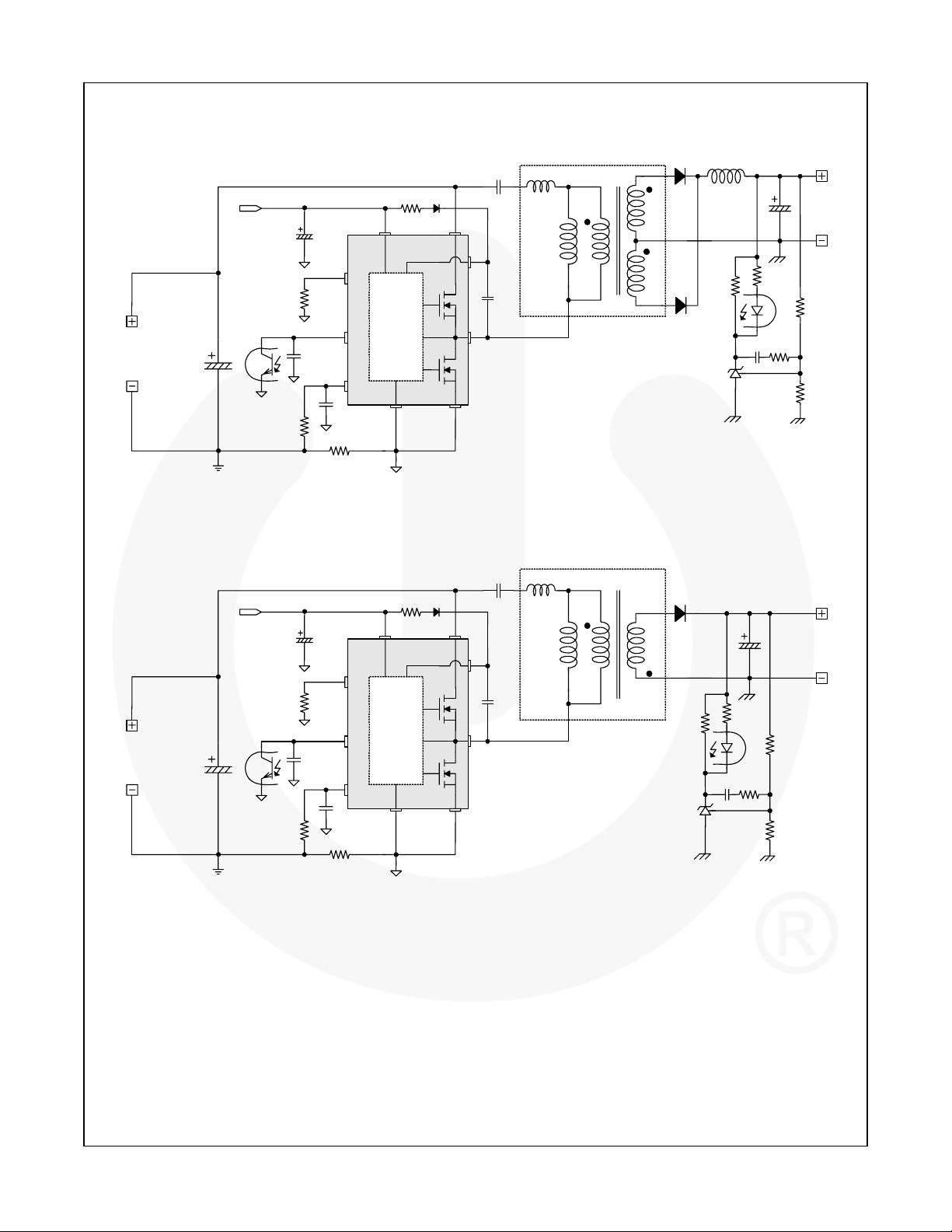
Figure 1. Typical Application Circuit for an Asymmetric PWM Half-Bridge Converter
C
B
Ns
D1
V
O
L
lk
Np
V
CC
LVcc
R
T
V
DL
Lm
HVcc
FB
sense
Control
IC
SG PG
V
CTR
R
C
F
F
KA431
C
DL
V
IN
V
CS
R
Figure 2. Typical Application Circuit for an Asymmetric PWM Flyback Converter
© 2008 Fairchild Semiconductor Corporation www.fairchildsemi.com
FSFA2100 • Rev. 1.0.0 2

Block Diagram
FSFA2100 — Fairchild Power Switch (FPS™) for Half-Bridge PWM Converter
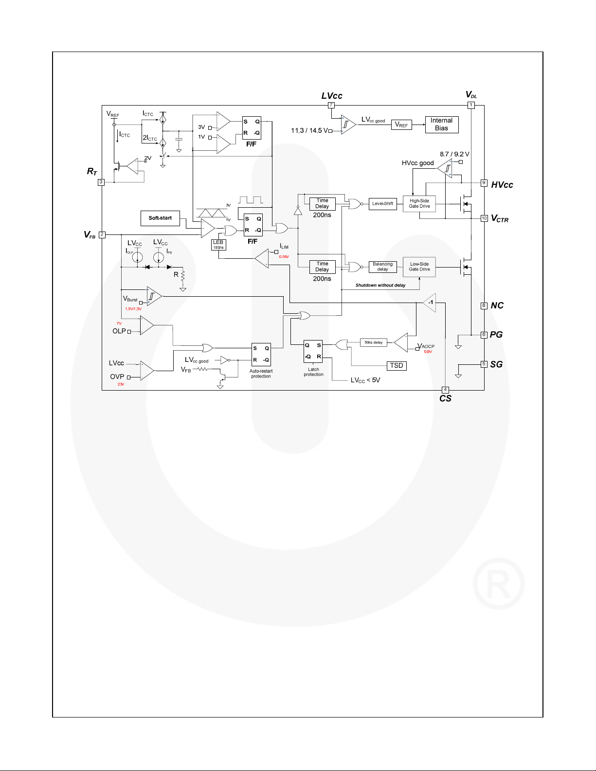
Figure 3. Internal Block Diagram
© 2008 Fairchild Semiconductor Corporation www.fairchildsemi.com
FSFA2100 • Rev. 1.0.0 3

Pin Configuration
1 2 3 4 5 6 7 8 9 10
CSSGPG
LVcc
HVcc
V
DL
R
T
V
FB
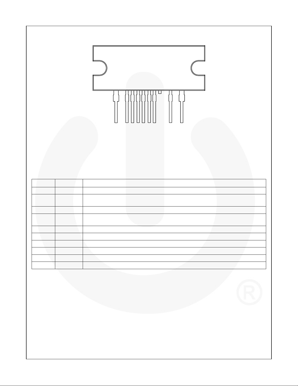
Figure 4. Package Diagram
FSFA2100 — Fairchild Power Switch (FPS™) for Half-Bridge PWM Converter
V
CTR
Pin Definitions
Pin # Name Description
1 VDL This is the drain of the high-side MOSFET, typically connected to the input DC link voltage.
2 VFB
3 RT This pin programs the switching frequency using a resistor.
4 CS
5 SG This pin is the control ground.
6 PG This pin is the power ground. This pin is connected to the source of the low-side MOSFET.
7 LVCC This pin is the supply voltage of the control IC.
8 NC No connection.
9 HVCC This is the supply voltage of the high-side gate-drive circuit IC.
10 V
CTR
This pin is connected to the inverting input of the PWM comparator internally and to the
opto-coupler externally. The duty cycle is determined by the voltage on this pin.
This pin senses the current flowing through the low-side MOSFET. Typically, negative
voltage is applied on this pin.
This is the drain of the low-side MOSFET. Typically, a transformer is connected to this pin.
© 2008 Fairchild Semiconductor Corporation www.fairchildsemi.com
FSFA2100 • Rev. 1.0.0 4

FSFA2100 — Fairchild Power Switch (FPS™) for Half-Bridge PWM Converter
Absolute Maximum Ratings
Stresses exceeding the absolute maximum ratings may damage the device. The device may not function or be
operable above the recommended operating conditions and stressing the parts to these levels is not recommended. In
addition, extended exposure to stresses above the recommended operating conditions may affect device reliability.
The absolute maximum ratings are stress ratings only. T
Symbol Parameter Min. Max. Unit
VDS Maximum Drain-to-Source Voltage (VDL-V
LVCC Low-Side Supply Voltage -0.3 25.0 V
HVCC to V
HVCC High-Side Floating Supply Voltage -0.3 625.0 V
VFB Feedback Pin Input Voltage -0.3 LVCC V
VCS Current Sense (CS) Pin Input Voltage -5.0 1.0 V
VRT R
dV
CTR
PD Total Power Dissipation
TJ
T
MOSFET Section
V
DGR
VGS Gate Source (GND) Voltage ±30 V
IDM Drain Current Pulsed 33 A
Package Section
Torque Recommended Screw Torque 5~7 kgf·cm
Notes:
3. Per MOSFET when both MOSFETs are conducting.
4. The maximum value of the recommended operating junction temperature is limited by thermal shutdown.
High-Side VCC Pin to Low-Side Drain Voltage -0.3 25.0 V
CTR
Pin Input Voltage -0.3 5.0 V
T
/dt Allowable Low-Side MOSFET Drain Voltage Slew Rate 50 V/ns
(3)
12.0 W
Maximum Junction Temperature
(4)
Recommended Operating Junction Temperature
Storage Temperature Range -55 +150
STG
Drain Gate Voltage (RGS=1MΩ)
ID Continuous Drain Current
=25°C unless otherwise specified.
A
and V
CTR
+150
(4)
) 600 V
CTR-PG
-40 +130
°C
°C
600 V
TC=25°C
T
=100°C
C
11
7
A
Thermal Impedance
TA=25°C unless otherwise specified.
Symbol Parameter Value Unit
θJC Junction-to-Case Center Thermal Impedance (Both MOSFETs Conducting) 10.44 ºC/W
© 2008 Fairchild Semiconductor Corporation www.fairchildsemi.com
FSFA2100 • Rev. 1.0.0 5
 Loading...