Fairchild FSEZ1307 service manual

February 2010
FSEZ1307
Primary-Side-Regulation PWM with Power MOSFET
Integrated
FSEZ1307 — Primary-Side-Regulation PWM with Power MOSFET Integrated
Features
Low Standby Power: Under 30mW
High-Voltage Startup
Few External Components
Constant-Voltage (CV) and Constant-Current (CC)
Control without Secondary-Feedback Circuitry
Green Mode: Linearly Decreasing PWM Frequency
Fixed PWM Frequency at 50kHz with Frequency
Hopping to Solve EMI Problem
Cable Compensation in CV Mode
Peak-Current-Mode Control in CV Mode
Cycle-by-Cycle Current Limiting
V
V
Over-Voltage Protection with Auto Restart
DD
Under-Voltage Lockout (UVLO)
DD
Gate Output Maximum Voltage Clamped at 15V
Fixed Over-Temperature Protection with
Auto Restart
Available in 7-Lead SOP Package
Applications
Description
This third-generation Primary Side Regulation (PSR)
PWM controller combination power MOSFET,
FSEZ1307, provides several features to enhance the
performance of low-power flyback converters. The
proprietary topology, TRUECURRENT™, enables
precise CC regulation and simplified circuit design for
battery-charger applications. Compared to a
conventional design or a linear transformer, a low-cost,
smaller, and
To minimize standby power consumption, the
proprietary green mode provides off-time modulation to
linearly decrease PWM frequency under light-load
conditions. Green mode assists the power supply in
meeting power conservation requirements.
By using the FSEZ1307, a charger can be implemented
with few external components and minimized cost. A
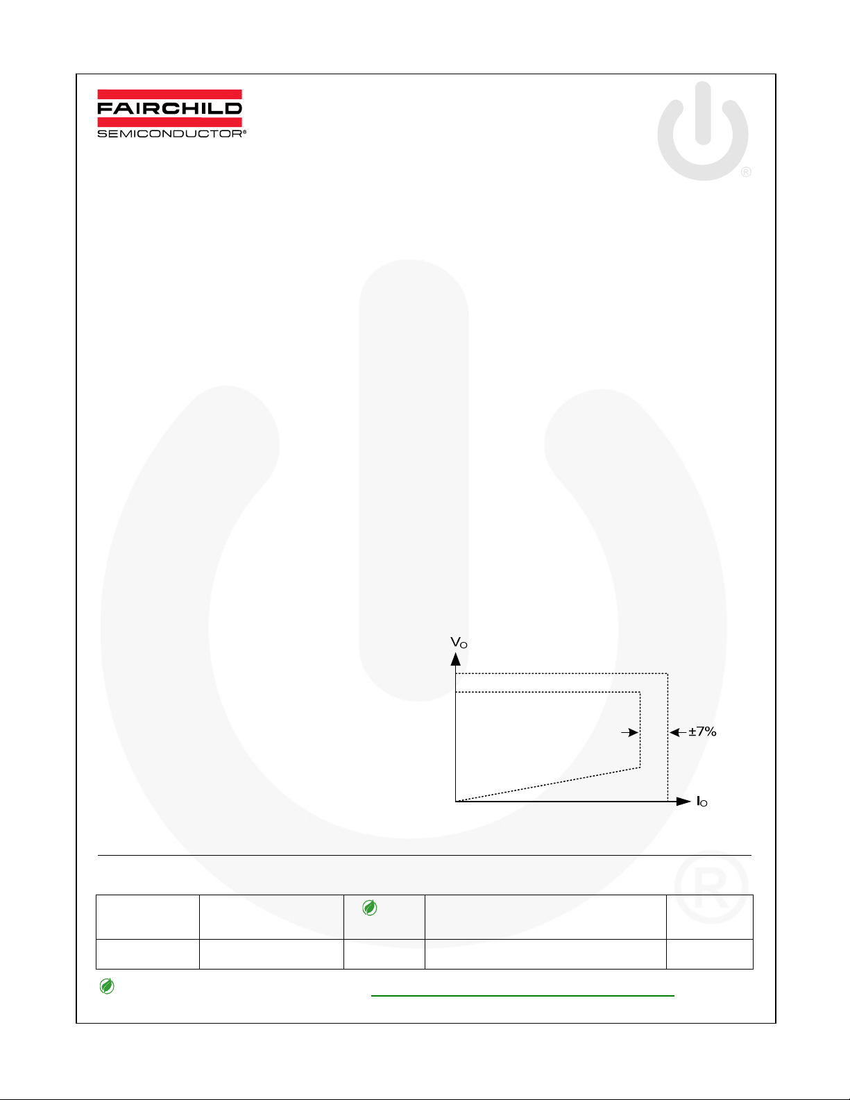
typical output CV/CC characteristic envelope is shown
in Figure 1.
lighter charger results.
Battery chargers for cellular phones, cordless
phones, PDA, digital cameras, power tools, etc.
Replaces linear transformers and RCC SMPS
Figure 1. Typical Output V-I Characteristic
Ordering Information
Part Number
FSEZ1307MY -40°C to +105°C Green 7-Lead, Small Outline Package (SOP-7) Tape & Reel
For Fairchild’s definition of Eco Status, please visit: http://www.fairchildsemi.com/company/green/rohs_green.html.
© 2010 Fairchild Semiconductor Corporation www.fairchildsemi.com
FSEZ1307 • Rev. 1.0.2
Operating
Temperature Range
Eco
Status
Package
Packing
Method

Application Diagram
AC
Input
D
1
R
F
D
2
D
4
D
3
FSEZ1307 — Primary-Side-Regulation PWM with Power MOSFET Integrated
C
R
sn2
L
1
R
sn2
R
C
1
C
2
D
C
VDD
VDD
2
DRAIN
HV
7
CS
COMR
3
GND
VS
sn1
C
sn
D
sn
Fa
C
VS
5
8
1
4
C
CR
R
R
R
T
1
2
SENSE
sn
1
D
F
DC
C
O1
R
C
d
O2
Output
Internal Block Diagram
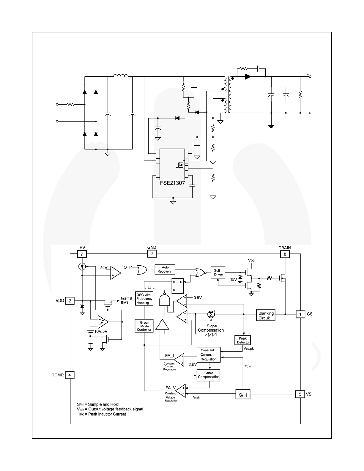
Figure 2. Typical Application
Figure 3. Functional Block Diagram
© 2010 Fairchild Semiconductor Corporation www.fairchildsemi.com
FSEZ1307 • Rev. 1.0.2 2

Marking Information
Pin Configuration
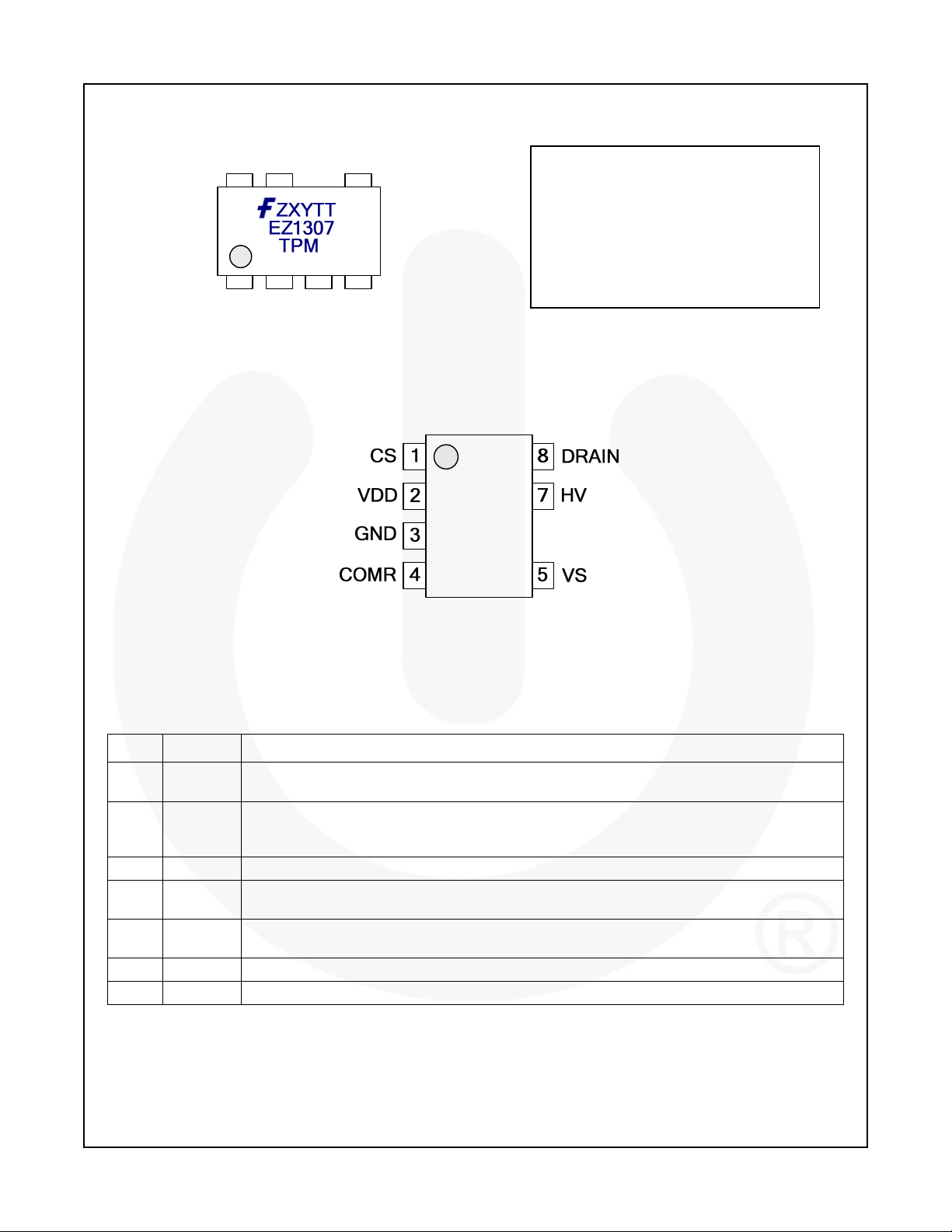
Figure 4. Top Mark
FSEZ1307 — Primary-Side-Regulation PWM with Power MOSFET Integrated
F: Fairchild Logo
Z: Plant Code
X: 1-Digit Year Code
Y: 1-Digit Week Code
TT: 2-Digit Die Run Code
T: Package Type (M=SOP)
P: Y=Green Package
M: Manufacture Flow Code
Pin Definitions
Pin # Name Description
1 CS
2 VDD
3 GND
4 COMR
5 VS
7 HV
8 DRAIN
Current Sense. This pin connects a current-sense resistor to detect the MOSFET current for
peak-current-mode control in CV mode and provides the output-current regulation in CC mode.
Power Supply. IC operating current and MOSFET driving current are supplied using this pin.
This pin is connected to an external VDD capacitor of typically 10µF. The threshold voltages for
startup and turn-off are 16V and 5V, respectively. The operating current is lower than 5mA.
Ground
Cable Compensation. This pin connects a 1µF capacitor between the COMR and GND pins
for compensation voltage drop due to output cable loss in CV mode.
Voltage Sense. This pin detects the output voltage information and discharge time based on
voltage of auxiliary winding.
High Voltage. This pin connects to a bulk capacitor for high-voltage startup.
Driver Output. Power MOSFET drain. This pin is the high-voltage power MOSFET drain.
Figure 5. Pin Configuration
© 2010 Fairchild Semiconductor Corporation www.fairchildsemi.com
FSEZ1307 • Rev. 1.0.2 3

FSEZ1307 — Primary-Side-Regulation PWM with Power MOSFET Integrated
Absolute Maximum Ratings
Stresses exceeding the absolute maximum ratings may damage the device. The device may not function or be
operable above the recommended operating conditions and stressing the parts to these levels is not recommended.
In addition, extended exposure to stresses above the recommended operating conditions may affect device reliability.
The absolute maximum ratings are stress ratings only.
Symbol Parameter Min. Max. Units
V
HV Pin Input Voltage 500 V
HV
V
DC Supply Voltage
VDD
VVS VS Pin Input Voltage -0.3 7.0 V
VCS CS Pin Input Voltage -0.3 7.0 V
V
Voltage Error Amplifier Output Voltage -0.3 7.0 V
COMV
V
Current Error Amplifier Output Voltage -0.3 7.0 V
COMI
VDS Drain-Source Voltage 700 V
ID Continuous Drain Current
IDM Pulsed Drain Current 3.5 A
EAS Single Pulse Avalanche Energy 35 mJ
IAR Avalanche Current 1 A
PD
θ
θJC
Power Dissipation (T
Thermal Resistance (Junction to Air) 150 °C/W
JA
Thermal Resistance (Junction to Case) 39 °C/W
TJ Operating Junction Temperature -40 +150 °C
T
Storage Temperature Range -55 +150 °C
STG
TL Lead Temperature (Wave Soldering or IR, 10 Seconds) +260 °C
ESD
Electrostatic Discharge
Capability
Notes:
1. Stresses beyond those listed under Absolute Maximum Ratings may cause permanent damage to the device.
2. All voltage values, except differential voltages, are given with respect to the GND pin.
(1,2)
30 V
T
=25°C 0.5 A
A
TA=100°C 0.35 A
<50°C)
A
Human Body Model (Except HV Pin),
JEDEC-JESD22_A114
Charged Device Model (Except HV Pin),
JEDEC-JESD22_C101
660 mW
2500
V
1250
Recommended Operating Conditions
The Recommended Operating Conditions table defines the conditions for actual device operation. Recommended
operating conditions are specified to ensure optimal performance to the datasheet specifications. Fairchild does not
recommend exceeding them or designing to Absolute Maximum Ratings.
Symbol Parameter Min. Max. Units
TA Operating Ambient Temperature -40 +105 °C
© 2010 Fairchild Semiconductor Corporation www.fairchildsemi.com
FSEZ1307 • Rev. 1.0.2 4

Electrical Characteristics
Unless otherwise specified, VDD=15V and TA=25℃.
Symbol Parameter Conditions Min. Typ. Max. Units
VDD Section
VOP Continuously Operating Voltage 23 V
V
Turn-On Threshold Voltage 15 16 17 V
DD-ON
V
Turn-Off Threshold Voltage 4.5 5.0 5.5 V
DD-OFF
I
DD-OP
I
DD-GREEN
V
DD-OVP
V
DD-OVP-HYS
t
D-VDDOVP
Operating Current
Green-Mode Operating Supply Current
VDD Over-Voltage-Protection Level (OVP) 24 V
Hysteresis Voltage for VDD OVP 1.5 2.0 2.5 V
VDD Over-Voltage-Protection Debounce Time 50 200 300 µs
HV Startup Current Source Section
V
Minimum Startup Voltage on HV Pin 50 V
HV-MIN
IHV Supply Current Drawn from HV Pin VDC=100V 1.5 3.0 mA
HV=500V,
I
Leakage Current after Startup
HV-LC
V
OFF
DD
= V
+1V
DD-
Oscillator Section
f
Frequency
OSC
f
OSC-N-MIN
f
OSC-CM-MIN
Minimum Frequency at No-Load 370 Hz
Minimum Frequency at CCM 13 kHz
Center Frequency 47 50 53
Frequency Hopping Range ±1.5 ±2.0 ±2.5
fDV Frequency Variation vs. VDD Deviation VDD=10~25V, 1 2 %
=-40°C to
T
fDT Frequency Variation vs. Temperature Deviation
A
105°C
Voltage-Sense Section
Itc IC Bias Current 10 µA
V
BIAS-COMV
Adaptive Bias Voltage Dominated by V
R
COMV
=20kΩ 1.4 V
VS
Current-Sense Section
tPD Propagation Delay to GATE Output
t
Minimum On Time at No-Load 700 850 1050 ns
MIN-N
VTH Threshold Voltage for Current Limit 0.8 V
Voltage-Error-Amplifier Section
VVR Reference Voltage 2.475 2.500 2.525 V
f
VN Green-Mode Starting Voltage on EA_V
VG Green-Mode Ending Voltage on EA_V f
-2kHz
OSC
=1kHz 0.4 V
OSC
Current-Error-Amplifier Section
VIR Reference Voltage 2.475 2.500 2.525 V
Cable Compensation Section
V
COMR Pin for Cable Compensation 0.75 V
COMR
2.5 5.0 mA
0.95 1.20 mA
0.96 3.00 µA
kHz
15 %
90 200 ns
2.5 V
FSEZ1307 — Primary-Side-Regulation PWM with Power MOSFET Integrated
Continued on the following page…
© 2010 Fairchild Semiconductor Corporation www.fairchildsemi.com
FSEZ1307 • Rev. 1.0.2 5
 Loading...