Fairchild FSEZ1216B service manual
January 2009
FSEZ1216B
Primary-Side-Regulation PWM Integrated Power MOSFET
FSEZ1216B — Primary-Side-Regulation PWM Integrated Power MOSFET
Features
Constant-Voltage (CV) and Constant-Current (CC)
Control without Secondary-Feedback Circuitry
Green-Mode Function: PWM Frequency Linearly
Decreasing
Fixed PWM Frequency at 50kHz with Frequency
Hopping to Solve EMI Problems
Cable Compensation in CV mode
Low Startup Current: 10μA
Low Operating Current: 3.5mA
Peak-Current-Mode Control in CV Mode
Cycle-by-Cycle Current Limiting
V
V
Over-Voltage Protection (OVP) with
DD
Auto-Restart
Under-Voltage Lockout (UVLO)
DD
Fixed Over-Temperature Protection (OTP)
with Latch
DIP-8 Package Available
Applications
Description
This highly integrated PWM controller provides several
features to enhance the performance of low-power
flyback converters. The proprietary topology enables
most simplified circuit design especially for battery
charger applications. A low-cost, smaller, and lighter
charger results when compared to a conventional
design or a linear transformer. The startup current is
only 10μA, which allows large startup resistance for
further power saving.
To minimize the standby-power consumption, the
proprietary green-mode function provides off-time
modulation to linearly decrease PWM frequency under
light-load conditions. This green-mode function assists
the power supply in meeting power conservation
requirements.
By using FSEZ1216B, a charger can be implemented
with few external components and minimized cost. A
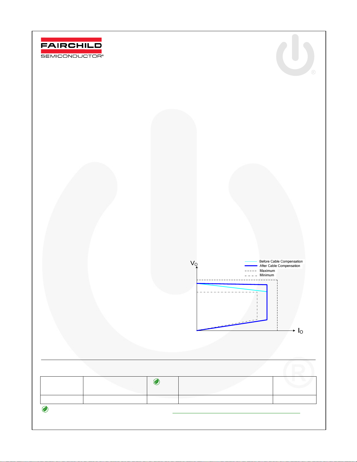
typical output CV/CC characteristic envelope is shown
in Figure 1.
FSEZ1216B series controllers are available in an 8-pin
DIP package.
Battery Chargers for Cellular Phones, Cordless
Phones, PDA, Digital Cameras, Power Tools
Best Choice to Replace Linear Transformer and
RCC SMPS
Figure 1. Typical Output V-I Characteristic
Ordering Information
Part Number
FSEZ1216BNY -40°C to +105°C Green 8-Lead, Dual Inline Package (DIP-8) Tube
For Fairchild’s definition of “green” Eco Status, please visit: http://www.fairchildsemi.com/company/green/rohs_green.html.
© 2008 Fairchild Semiconductor Corporation www.fairchildsemi.com
FSEZ1216B Rev. 1.0.0
Operating
Temperature Range
Eco
Status
Package
Packing
Method
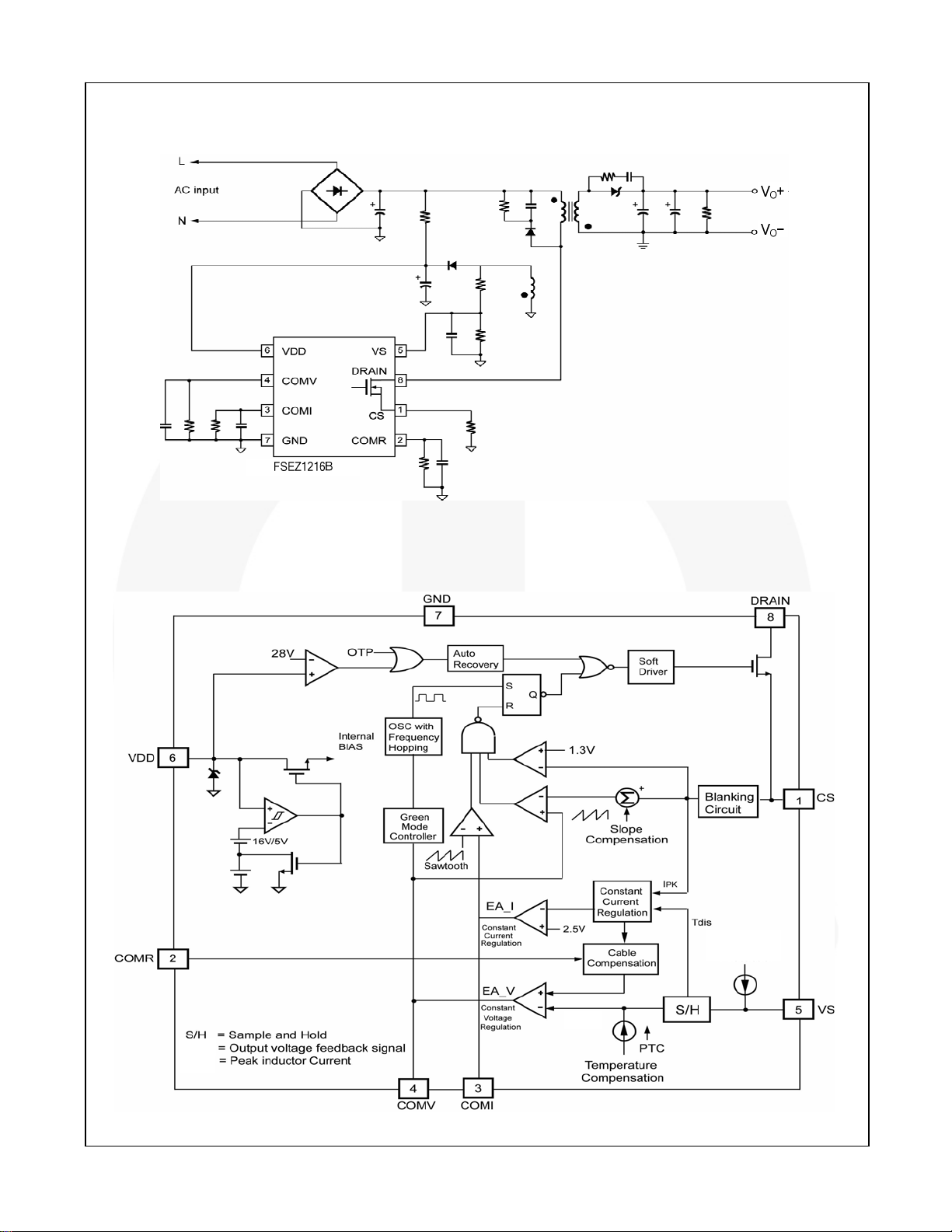
Application Diagram
FSEZ1216B — Primary-Side-Regulation PWM Integrated Power MOSFET
Figure 2. Typical Application
Internal Block Diagram
V
sah
I
PK
Brownout
Protection
V
sah
Figure 3. Functional Block Diagram
© 2008 Fairchild Semiconductor Corporation www.fairchildsemi.com
FSEZ1216B Rev. 1.0.0 2
Marking Information
DXYTT DXYTT
ZXYTT
EZ1216B
TPM
Pin Configuration
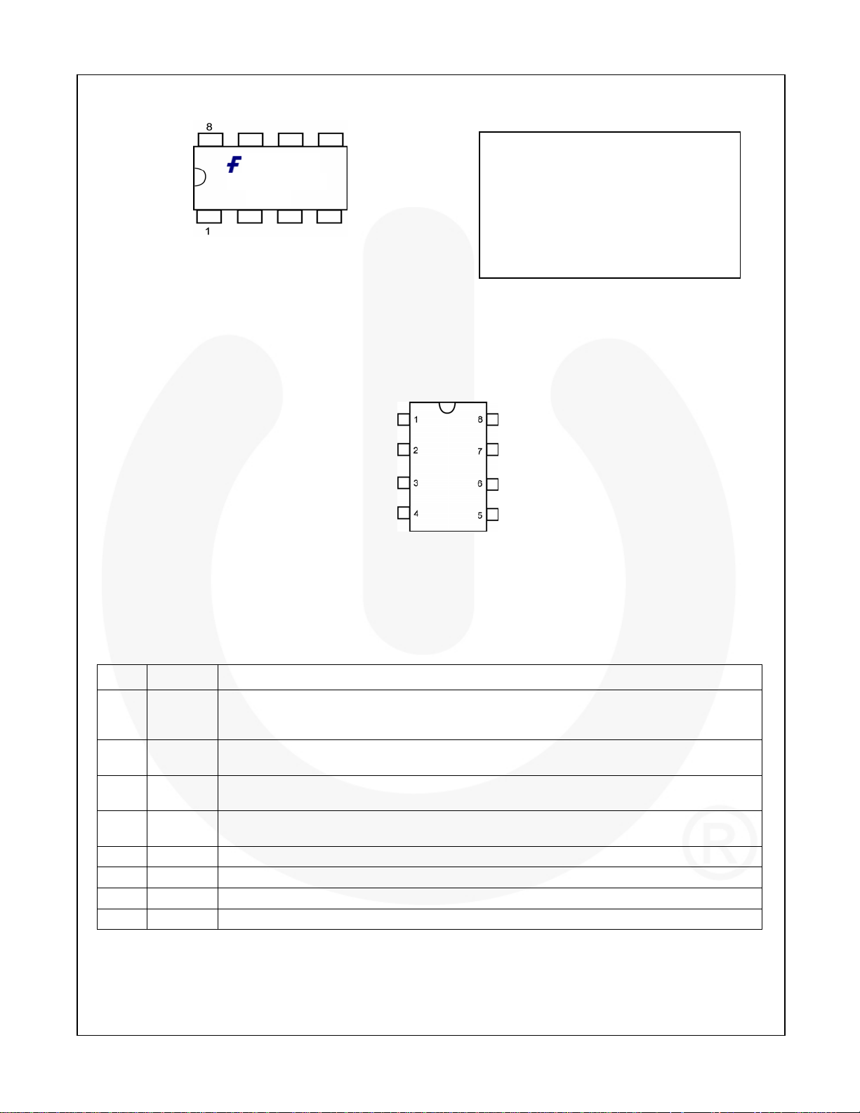
Figure 4. Top Mark
CS
FSEZ1216B — Primary-Side-Regulation PWM Integrated Power MOSFET
F- Fairchild Logo
Z- Plant Code
X- 1 Digit Year Code
Y- 1 Digit Week Code
TT: 2 Digits Die Run Code
T: Package Type (N=DIP)
P: Y: Green Package
M: Manufacture Flow Code
DRAIN
Pin Definitions
Pin # Name Description
Analog Input, Current Sense. Connected to a current-sense resistor for peak-current-mode
1 CS
2 COMR
3 COMI
4 COMV
5 VS
6 VDD Supply, Power Supply.
7 GND Voltage Reference, Ground.
8 DRAIN
control in CV mode. The current-sense signal is also provided for output-current regulation in
CC mode.
Analog Output, Cable Compensation. Connect a resistor between COMR and GND for cable
loss compensation in CV mode.
Analog Output, Current Compensation. Output of the current error amplifier. Connect a
capacitor between COMI pin and GND for frequency compensation.
Analog Output, Voltage Compensation. Output of the voltage error amplifier. Connect a
capacitor between COMV pin and GND for frequency compensation.
Analog Input, Voltage Sense. Output-voltage-sense input for output-voltage regulation.
Driver Output, Power MOSFET Drain. This pin is the high-voltage power MOSFET drain
COMR
COMI
COMV
Figure 5. Pin Configuration
GND
VDD
VS
© 2008 Fairchild Semiconductor Corporation www.fairchildsemi.com
FSEZ1216B Rev. 1.0.0 3
FSEZ1216B — Primary-Side-Regulation PWM Integrated Power MOSFET
Absolute Maximum Ratings
Stresses exceeding the absolute maximum ratings may damage the device. The device may not function or be
operable above the recommended operating conditions and stressing the parts to these levels is not recommended.
In addition, extended exposure to stresses above the recommended operating conditions may affect device reliability.
The absolute maximum ratings are stress ratings only.
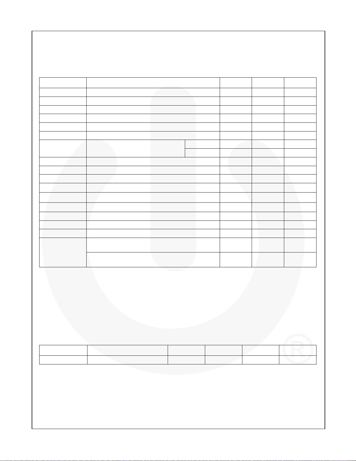
Symbol Parameter Min. Max. Unit
V
DC Supply Voltage
VDD
VVS VS Pin Input Voltage -0.3 7.0 V
VCS CS Pin Input Voltage -0.3 7.0 V
V
Voltage-Error Amplifier Output Voltage -0.3 7.0 V
COMV
V
Voltage-Error Amplifier Output Voltage -0.3 7.0 V
COMI
VDS Drain-Source Voltage 600 V
ID Continuous Drain Current
IDM Pulsed Drain Current 4 A
EAS Single-Pulse Avalanche Energy 33 mJ
IAR Avalanche Current 1 A
PD
Rθ
JA
RθJC
Power Dissipation (T
Thermal Resistance (Junction-to-Air) 113 °C/W
Thermal Resistance (Junction-to-Case) 67 °C/W
TJ Operating Junction Temperature +150 °C
T
Storage Temperature Range -55 +150 °C
STG
TL Lead Temperature (Wave Soldering or IR, 10 Seconds) +260 °C
Electrostatic Discharge Capability, Human Body Model,
ESD
JEDEC: JESD22-A114
Electrostatic Discharge Capability, Charged Device
Model, JEDEC: JESD22-C101
Notes:
1. Stresses beyond those listed under absolute maximum ratings may cause permanent damage to the device.
2. All voltage values, except differential voltages, are given with respect to GND pin.
(1,2)
30 V
TC=25°C 1 A
=100°C 0.6 A
T
C
<50°C)
A
800 mW
3.0 KV
1000 V
Recommended Operating Conditions
The Recommended Operating Conditions table defines the conditions for actual device operation. Recommended
operating conditions are specified to ensure optimal performance to the datasheet specifications. Fairchild does not
recommend exceeding them or designing to Absolute Maximum Ratings.
Symbol Parameter Min. Typ. Max. Unit
TA Operating Ambient Temperature -40 +105 °C
© 2008 Fairchild Semiconductor Corporation www.fairchildsemi.com
FSEZ1216B Rev. 1.0.0 4
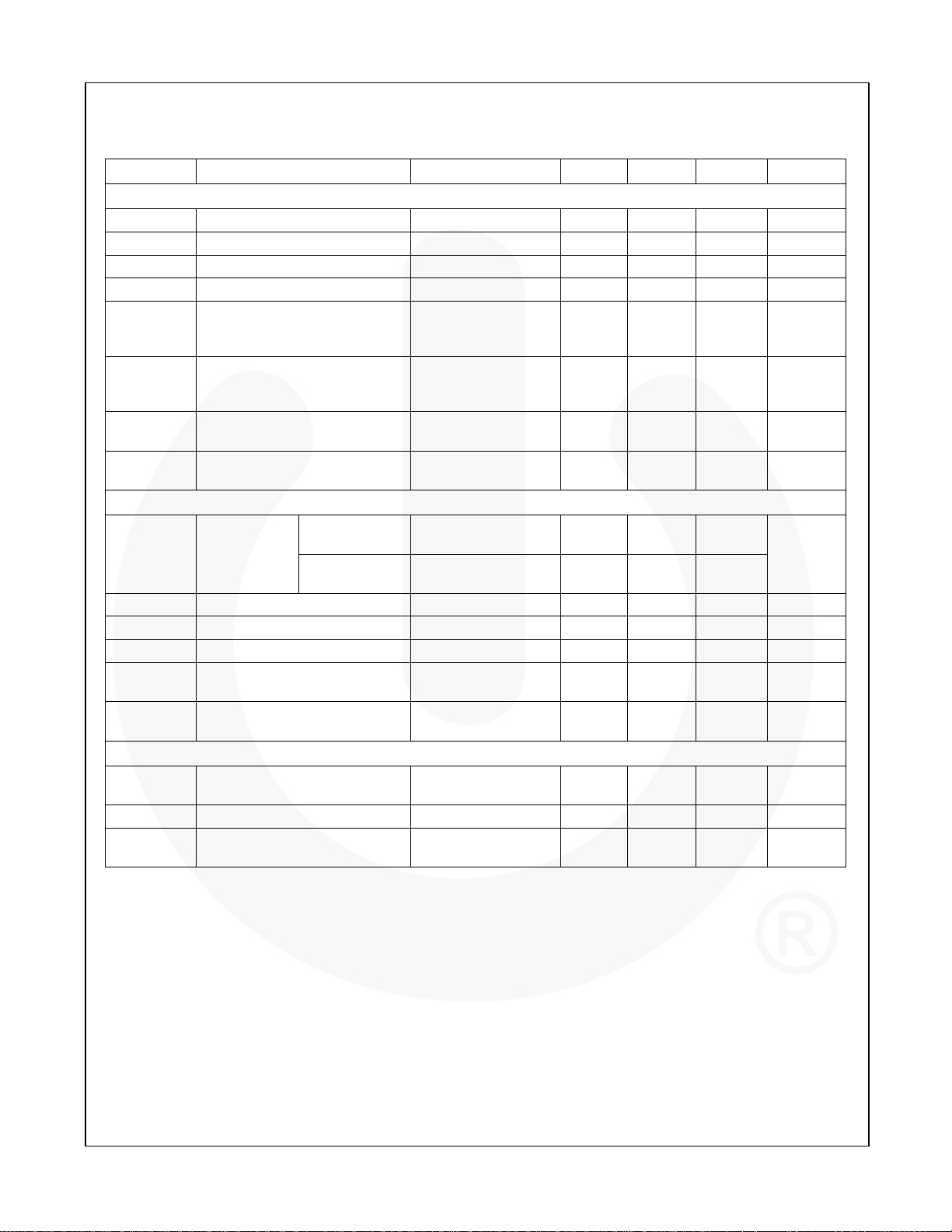
Electrical Characteristics
VDD=15V, TA=25°C, unless otherwise specified.
Symbol Parameter Conditions Min. Typ. Max. Units
VDD SECTION
VOP Continuously Operating Voltage 25 V
V
Turn-On Threshold Voltage 15 16 17 V
DD-ON
V
Turn-Off Threshold Voltage 4.5 5.0 5.5 V
DD-OFF
I
Startup Current 0<VDD<V
DD-ST
V
=20V, fS=f
I
Operating Current
DD-OP
I
DD-GREEN
V
DD-OVP
t
D-VDDOVP
Green-Mode Operating Supply
Current
Over-Voltage-Protection
V
DD
Level
Over-Voltage-Protection
V
DD
Debounce Time
DD
VVS=2V, VCS=3V,
C
=1nF
L
=20V, VVS=2.7V
V
DD
=0V, V
V
CS
f
S=fOSC-N-MIN
=2.3V, VCS=3V 27 28 29 V
V
VS
f
S=fOSC
OSCILLATOR SECTION
Center
f
Frequency
OSC
Frequency
FrequencyHopping Range
t
Frequency-Hopping Period VCS=1.5V, VVS=2V 2.56 ms
FHR
f
OSC-N-MIN
f
OSC-CM-MIN
Minimum Frequency at No-Load VVS=2.7V, V
Minimum Frequency at CCM VVS=2.3V, VCS=0.5V 18 KHz
fDV
fDT
Frequency Variation vs. V
Deviation
Frequency Variation vs.
Temperature Deviation
DD
=25°C, VVS=2.3V 48 50 55
T
A
=1.5V, VVS=2V ±1.0 ±1.5 ±2.3
V
CS
=10V to 25V 5 %
V
DD
=-40°C to 105°C 15 %
T
A
VOLTAGE-SENSE SECTION
I
VS-UVP
Itc IC Compensation Bias Current 9.5 μA
V
BIAS-COMV
Sink Current for Brownout
Protection
Adaptive Bias Voltage
Dominated by V
COMV
=20KΩ 125 μA
R
VS
=0V,RVS=20KΩ 1.4 V
V
COMV
-0.16V 10 20 μA
DD-ON
,
OSC
3.5 5.0 mA
COMV
=0V
1 2 mA
, CL=1nF
, VVS=2.3V 100 250 400 μs
KHz
=0V 500 Hz
COMV
FSEZ1216B — Primary-Side-Regulation PWM Integrated Power MOSFET
© 2008 Fairchild Semiconductor Corporation www.fairchildsemi.com
FSEZ1216B Rev. 1.0.0 5
 Loading...