Fairchild FSEZ1216 service manual

April 2009
FSEZ1216 — Primary-Side-Regulation PW M Integrated
Power MOSFET
FSEZ1216 — Primary-Side-Regulation PWM Integrated Power MOSFET
Features
Constant-Voltage (CV) and Constant-Current (CC)
Control without Secondary-Feedback Circuitry
Green Mode: Frequency Reduction at Light-Load
Fixed PWM Frequency at 42kHz with Frequency
Hopping to Reduce EMI
Cable Voltage Drop Compensation in CV Mode
Low Startup Current: 10μA
Low Operating Current: 3.5mA
Peak-Current-Mode Control in CV Mode
Cycle-by-Cycle Current Limiting
V
V
Over-Voltage Protection with Auto-Restart
DD
Under-Voltage Lockout (UVLO)
DD
Gate Output Maximum Voltage Clamped at 18V
Fixed Over-Temperature Protection with Latch
DIP-8 Package Available
Applications
Battery Chargers for Cellular Phones, Cordless
Phones, PDA, Digital Cameras, Power Tools
Description
The primary-side PWM integrated Power MOSFET,
FSEZ1216, significantly simplifies power supply design
that requires CV and CC regulation capabilities.
FSEZ1216 controls the output voltage and current
precisely only with the information in the primary side of
the power supply, not only removing the output current
sensing loss, but also eliminating all secondary
feedback circuitry.
The green-mode function with a low startup current
(10µA) maximizes the light load efficiency so the power
supply can meet stringent standby power regulations.
Compared with conventional secondary side regulation
approach, the FSEZ1216 can reduce total cost,
component count, size, and weight, while
simultaneously increasing efficiency, productivity, and
system reliability.
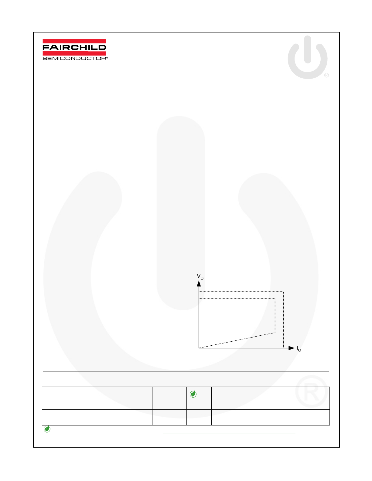
A typical output CV/CC characteristic envelope is shown
in Figure 1.
Replaces Linear Transformer and RCC SMPS
Offline High Brightness (HB) LED Drivers
Figure 1. Typical Output V-I Characteristic
Ordering Information
Operating
Part Number
FSEZ1216NY -40°C to +105°C 600V
For Fairchild’s definition of Eco Status, please visit: http://www.fairchildsemi.com/company/green/rohs_green.html.
© 2009 Fairchild Semiconductor Corporation www.fairchildsemi.com
FSEZ1216 • Rev. 1.0.1
Temperature
Range
MOSFET
BV
DSS
MOSFET
R
DS.ON
9.3Ω
(Typical)
Eco
Status
Green 8-Lead, Dual Inline Package (DIP-8) Tube
Package
Packing
Method

Application Diagram
Bridge
Rectifier
Diode
FSEZ1216 — Primary-Side-Regulation PWM Integrated Power MOSFET
R
C
SN2
SN2
V
O
R
D
DD
SN1CSN1
D
SN
N
P
V
DL
+
R
C
DL
-
START
D
R
N
S
C
O
I
O
ACLine
R
CS
C
COMR
R
COMR
C
COMI
R
COMI
Internal Block Diagram
VDD
6
GND
+
-
16V/5V
OSC with
Frequency
Hopping
Green Mode
Controller
7
Internal Bias
C
FSEZ1216
CS
1
2
COMR
COMI
3
COMV
4 5
C
COMV
R
COMV
DRAIN
GND
VDD
VS
8
7
6
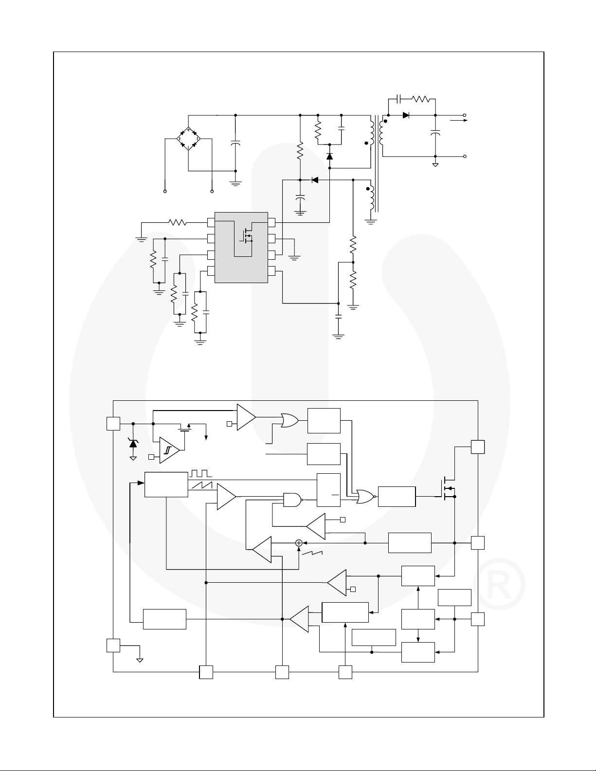
Figure 2. Typical Application
+
OVP
-
28V
Brownout
OTP
-
+
PWM
Comparator
Comparator
PWM
Comparator
-
+
PWM
Slope Compensation
+
-
EA_V
DD
C
Auto
Restart
Prote ction
Latch
Prote ction
SRQ
+
-
EA_I
Compensation
S
Q
1.3V
-
+
Cable Drop
N
A
R
S1
R
S2
Soft-Driver
2.5V
Temperature
Compensation
Leading-Edge
Blanking
I
O
Estima tor
t
DIS
Detector
V
O
Estima tor
Brownout
Protection
8
1
5
DRAIN
CS
VS
3
COMI
4
COMV
2
COMR
Figure 3. Functional Block Diagram
© 2009 Fairchild Semiconductor Corporation www.fairchildsemi.com
FSEZ1216 • Rev. 1.0.1 2

Marking Information
Pin Configuration
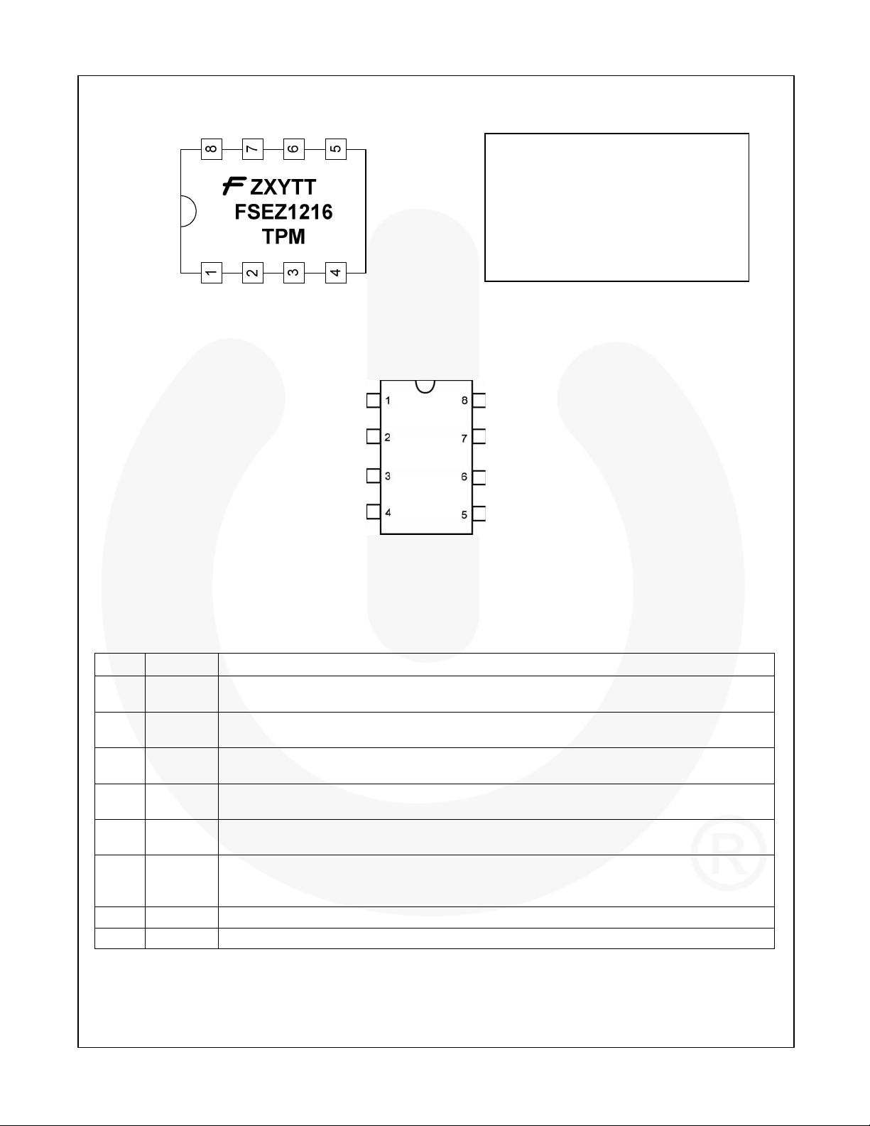
Figure 4. Top Mark
FSEZ1216 — Primary-Side-Regulation PWM Integrated Power MOSFET
F- Fairchild Logo
Z- Plant Code
X- 1-Digit Year Code
Y- 1-Digit Week Code
TT- 2-Digits Die Run Code
T- Package Type (N=DIP)
P- Z: Pb Free, Y: Green Package
M- Manufacture Flow Code
Pin Definitions
Pin # Name Description
1 CS
2 COMR
3 COMI
4 COMV
5 VS
6 VDD
7 GND
8 DRAIN
Current Sense. This pin connects a current-sense resistor to sense the MOSFET current for
peak-current-mode control in CV mode and provides for output-current regulation in CC mode.
Cable Compensation. This pin connects a capacitor between COMR and GND for
compensation voltage drop due to output cable loss in CV mode.
Constant Current Loop Compensation. This pin connects a capacitor and a resistor between
COMI and GND for compensation current loop gain.
Constant Voltage Loop Compensation. This pin connects a capacitor and a resistor between
COMV and GND for compensation voltage loop gain.
Voltage Sense. This pin detects the output voltage information and discharge time based on
voltage of auxiliary winding. This pin connects two divider resistors and one capacitor.
Power Supply. The power supply pin for the IC operating current and MOSFET driving current.
This pin is connects to an external VDD capacitor (typically 10μF). The threshold voltages for
startup and turn-off are 16V and 5V, respectively.
Ground.
Drain. This pin is the high-voltage power MOSFET drain.
CS
COMR
COMI
COMV
DRAIN
GND
VDD
VS
Figure 5. Pin Configuration
© 2009 Fairchild Semiconductor Corporation www.fairchildsemi.com
FSEZ1216 • Rev. 1.0.1 3

FSEZ1216 — Primary-Side-Regulation PWM Integrated Power MOSFET
Absolute Maximum Ratings
Stresses exceeding the absolute maximum ratings may damage the device. The device may not function or be
operable above the recommended operating conditions and stressing the parts to these levels is not recommended.
In addition, extended exposure to stresses above the recommended operating conditions may affect device reliability.
The absolute maximum ratings are stress ratings only.
Symbol Parameter Min. Max. Unit
V
DC Supply Voltage
VDD
VVS VS Pin Input Voltage -0.3 7.0 V
VCS CS Pin Input Voltage -0.3 7.0 V
V
Voltage Error Amplifier Output Voltage -0.3 7.0 V
COMV
V
Voltage Error Amplifier Output Voltage -0.3 7.0 V
COMI
VDS Drain-Source Voltage 600 V
ID Continuous Drain Current
IDM Pulsed Drain Current 4 A
EAS Single Pulse Avalanche Energy 33 mJ
IAR Avalanche Current 1 A
PD Power Dissipation (TA<50°C) 800 mW
Θ
JA
ΘJC
Thermal Resistance Junction-to-Air 113 °C/W
Thermal Resistance Junction-to-Case 67 °C/W
TJ Operating Junction Temperature +150 °C
T
Storage Temperature Range -55 +150 °C
STG
TL Lead Temperature (Wave Soldering or IR, 10 Seconds) +260 °C
Electrostatic Discharge Capability, Human Body Model,
ESD
JEDEC: JESD22-A114
Electrostatic Discharge Capability, Charged Device
Model, JEDEC: JESD22-C101
Note:
1. All voltage values, except differential voltages, are given with respect to GND pin.
(1)
30 V
TC=25°C 1.0
=100°C 0.6
T
C
A
2.5 KV
1250 V
Recommended Operating Conditions
The Recommended Operating Conditions table defines the conditions for actual device operation. Recommended
operating conditions are specified to ensure optimal performance to the datasheet specifications. Fairchild does not
recommend exceeding them or designing to Absolute Maximum Ratings.
Symbol Parameter Conditions Min. Typ. Max. Unit
TA Operating Ambient Temperature -40 +105 °C
© 2009 Fairchild Semiconductor Corporation www.fairchildsemi.com
FSEZ1216 • Rev. 1.0.1 4

Electrical Characteristics
VDD=15V and TA=25°C unless otherwise specified.
Symbol Parameter Conditions Min. Typ. Max. Units
VDD Section
VOP Continuously Operating Voltage 25 V
V
Turn-On Threshold Voltage 15 16 17 V
DD-ON
V
Turn-Off Threshold Voltage 4.5 5.0 5.5 V
DD-OFF
I
Startup Current 0< VDD < V
DD-ST
=20V, fS=f
V
I
Operating Current
DD-OP
I
DD-GREEN
V
DD-OVP
t
D-VDDOVP
Green Mode Operating Supply
Current
Over-Voltage Protection
V
DD
Level
Over-Voltage Protection
V
DD
Debounce Time
DD
V
=3V, CL=1nF
CS
=20V, VVS=2.7V,
V
DD
f
S=fOSC-N-MIN
V
=0V
COMV
V
=3V, VVS=2.3V,
CS
fs= f
, VVS=2.3V
OSC
Oscillator Section
f
Frequency
OSC
t
Frequency Hopping Period
FHR
f
OSC-N-MIN
f
OSC-CM-MIN
Minimum Frequency at No Load VVS=2.7V, V
Minimum Frequency at CCM VVS=2.3V, VCS=0.5V 20 KHz
fDV
fDT
Frequency Variation vs. V
Deviation
Frequency Variation vs.
Temperature Deviation
Center Frequency
Frequency
Hopping Range
DD
T
=25°C
A
=25°C
T
A
T
=25°C
A
V
=10V to 25V 5 %
DD
TA=-40°C to +85°C 15 %
Voltage-Sense Section
I
VS-UVP
Itc IC Compensation Bias Current 9.5 μA
V
BIAS-COMV
Sink Current for Brownout
Protection
Adaptive Bias Voltage
Dominated by V
COMV
RVS=20KΩ 180 μA
=0V, TA=25°C, RVS=20KΩ 1.4 V
V
COMV
Current-Sense Section
tPD
t
MIN-N
t
MINCC
D
SAW
VTH
Propagation Delay to GATE
Output
100 200 ns
Minimum On Time at No Load VVS=-0.8V, RS=2KΩ, V
Minimum On Time in CC Mode VVS=0V, V
Duty Cycle of SAW Limiter
Threshold Voltage for Current
Limit
1.3 V
-0.16V 0 1.6 10.0 μA
DD-ON
, VVS=2V,
OSC
, VCS=0V, CL=1nF,
3.5 5.0 mA
1 2 mA
27 28 29 V
100 250 400 μs
39 42 45
±1.8 ±2.6 ±3.6
3 ms
=0V 550 Hz
COMV
=1V 1100 ns
COMV
=2V 400 ns
COMV
40 %
Continued on following page…
FSEZ1216 — Primary-Side-Regulation PWM Integrated Power MOSFET
KHz
© 2009 Fairchild Semiconductor Corporation www.fairchildsemi.com
FSEZ1216 • Rev. 1.0.1 5
 Loading...