

www.fairchildsemi.com
Application Note AN4140
Transformer Design Consideration for off-line Flyback
Converters using Fairchild Power Switch (FPS
1. Introduction
For flyback coverters, the transformer is the most important
factor that determines the performance such as the
efficiency, output regulation and EMI. Contrary to the
normal transformer, the flyback transformer is inherently an
inductor that provides energy storage, coupling and isolation
for the flyback converter. In the general transformer, the
current flo ws in bot h the prim ary and se condary wi nding at
the same time. However, in the flyback transformer, the
current flows only in the primary winding while the energy
in the core is charged and in the secondary windin g while the
energy in the core is discharged. Usually gap is introduced
between the core to increase the energy storage capacity.
This paper presents practical design considerations of
transformers for off-line flyback converters employing
Fairchild Power Switch (FPS). In order to give insight to th e
reader, practical design examples are also provided.
2. General Transformer design procedure
(1) Choose the proper core
Core type
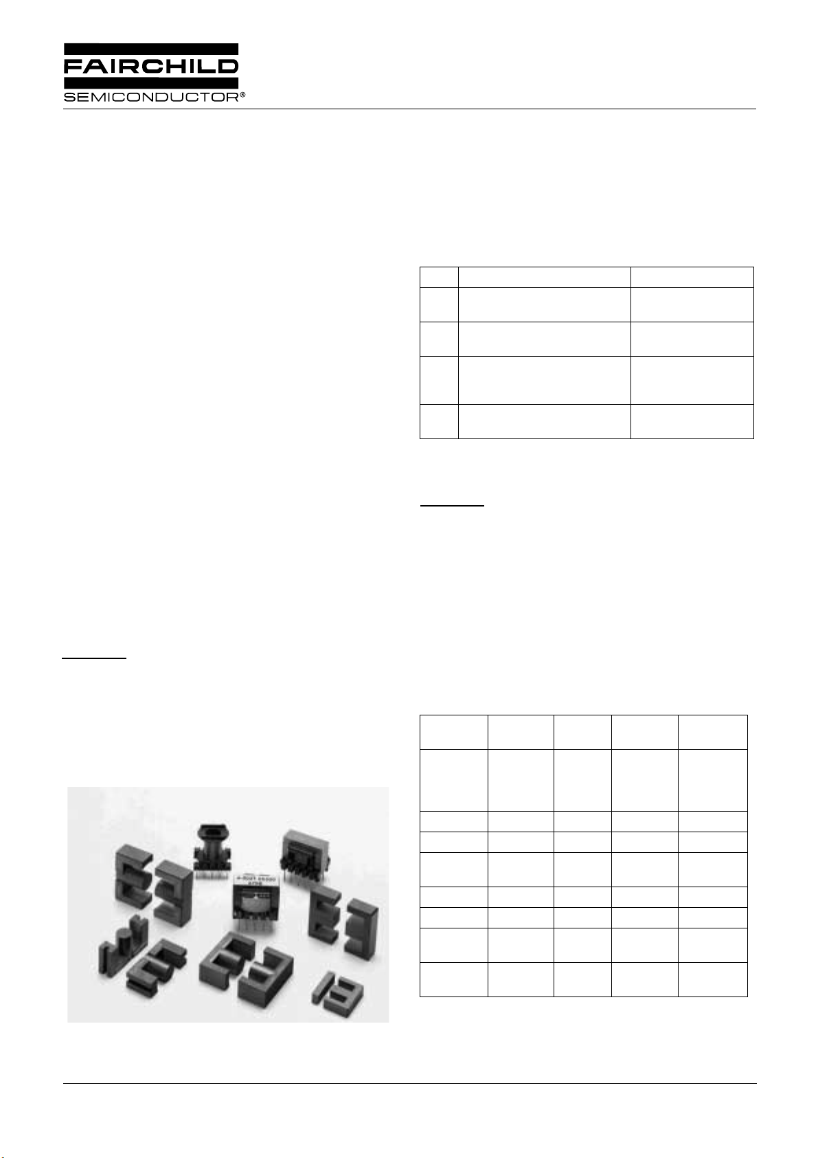
for commercial SMPS (Switchied mode power supply)
applications. Various ferrite cores and bobbins are shown in
Figure 1. The type of the core should be chosen with regard
to system requirements including number of outputs,
physical height, cost and so on. Table 1 shows features and
typical application of various cores.
: Ferrite is the most widely used core material
Core Features Typical Applications
EEEI-Low cost Aux. power
EFD
-Low profile LCD Monitor
EPC
EER -Large winding window area
-Various bobbins for multiple
output
PQ -Large cross sectional area
-Relatively expensive
Table 1. Features and typical applications of various
cores
Core size : Actually, the initial selection of the core is
bound to be crude since there are too many variables. One
way to select the proper core is to refer to the manufacture's
core selection guide. If there is no proper reference, use the
table 2 as a starting point. The core recommended in table 1
is typical for the universal input range, 67kHz switching
frequency and 12V singl e outp ut app lication . When th e in put
voltage range is 195-265 Vac (European input range) or the
switching frequency is higher than 67 kHz, a small er core can
be used. For an application with low voltage and/or mul tiple
outputs, usually a larger core should be used than
recommended in the table.
Output
Power
0-10W EI12.5
10-20W EI22 EE19 EPC19
20-30W EI25 EE22 EPC25 EER25.5
30-50W EI28
50-70W EI35 EE30 EER28L
70-100W EI40 EE35 EER35
100-150W EI50 EE40 EER40
150-200W EI60 EE50
EI core EE core EPC core EER core
EE8
EI16
EI19
EI30
EE10
EE13
EE16
EE25 EPC30 EER28
EE60
TM
)
Battery charger
CRT monitor, C-TV
DVDP, STB
EPC10
EPC13
EPC17
EER42
EER49
Figure 1. Ferrite core (TDK)
©2003 Fairchild Semiconductor Corporation
Table 2. Core quick selection table (For universal input
range, fs=67kHz and 12V single output)
Rev. 1.0.0
AN4140 APPLICATION NOTE
I
∆
∆
I
∆
∆
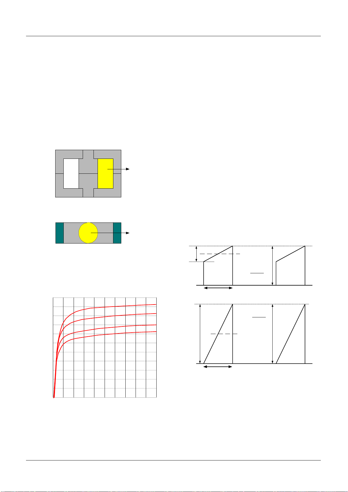
Once the core type and size are determined, the following
variables are obtained from the core data sheet.
- A
: The cross-sectional area of the core (mm2)
e
- A
: Winding window area (mm2)
w
- B
: Core saturation flux density (tesla)
sat
Figure 2 shows the Ae and A
of a core. The typical B-H
w
characteristics of ferrite core from TDK (PC40) are shown in
Figure 3. Since the saturation flux density (B
) decreases as
sat
the temperature increases, the high temperature characteristics should be considered. If there is no reference data, use
B
=0.3~0.35 T.
sat
Aw
Aw
AwAw
Ae
Ae
AeAe
(2) Determine the primary side inductance (Lm) of
the transformer
In order to determine the primary side inductance, the
following variables should be determined first. (For a
detailed design procedure, please refer to the application
note AN4137.)
- P
: Maximum input power
in
- f
: Switching frequency of FPS device
s
min
- V
- D
- K
: Minimum DC link voltage
DC
: Maximum duty cycle
max
: Ripple factor, which is defined at the minimum input
RF
voltage and full load condition, as shown in Figure 4. For
DCM opera tion, K
= 1 and for CCM operation KRF < 1.
RF
The ripple factor is closely related with the transformer size
and the RMS value of the MOSFET current. Even though
the conduction loss in the MOSFET can be reduced through
reducing the ripple factor, too small a ripple factor forces an
increase in transformer size. Considering both efficiency and
core size, it is reasonable to set K
universal input range and K
= 0.4-0.8 for the European
RF
= 0.3-0.5 for the
RF
input range. Meanwhile, in the case of low power
applications below 5W where size is most critical, a
relatively large ripple factor is used in order to minimize the
transformer size. In that case, it is typical to set K
0.7 for the universal input range and K
= 1.0 for the
RF
= 0.5-
RF
European input range.
Figure 2. Window Area and Cross Sectional Area
Magnetization Curves (typical)
Material :PC40
500
400
300
200
Flux density B (mT)
100
0
0
Figure 3. Typical B-H characteristics of ferrite core
(TDK/PC40)
800 1600
Magnetic field H (A/m)
25 ℃℃℃℃
60 ℃℃℃℃
100 ℃℃℃℃
120 ℃℃℃℃
peak
I
I
EDC
I
ds
peak
I
ds
I
EDC
=
K
RF
I
2
EDC
D
max
D
max
Figure 4. MOSFET Drain Current and Ripple Factor (KRF)
CCM operation : KRF < 1
K
=
RF
2
I
I
EDC
DCM operation : KRF =1
With the given variables, the primary side inductance, Lm is
obtained as
min
V
()
L
m
DC
--------------------------------------------- -= (1)
2PinfsK
2
D
⋅
max
RF
2
©2002 Fairchild Semiconductor Corporation
APPLICATION NOTE AN4140
I
I
where V
maximum duty cycle, P
the switching frequency of the FPS device and K
min
is the minimum DC input voltage, D
DC
is the maximum input power, fs is
in
max
RF
is the
is the
ripple factor.
Once L
is determined, the maximum peak cur rent and RMS
m
current of the MOSFET in normal operation are obtained as
peak
I
ds
rms
I
ds
where I
and
3I
()
∆
I
∆
I
-----+= (2)
I
EDC
2
2
2
+
EDC
------------------------------------- -=4()
EDC
V
min
V
DC
-----------------------------------= (5)
Lmf
D
∆
I
DC
D
s
max
-----
------------- -=3()
2
3
P
in
min
D
⋅
max
max
With the chosen core, the minimum number of turns for the
transformer primary side to avoid the core saturation is given
by
LmI
min
N
P
over
-------------------
= (6)
B
satAe
10
×
6
(turns)
(3) Determine the number of turns for each output
Figure 6 shows the simplified diagram of the transformer,
whrere V
by the feedback control while V
stands for the reference output th at is regulated
o1
stands for the n-th
o(n)
output.
First, determine the turns ratio (n) between the primary side
and the feedback controlled secondary side as a reference.
V
R0
--------------------------
n
Vo1VF1+
where N
and Ns1 are the number of turns for primary side
p
and reference output, respectively, V
and V
is the diode (DR1) forward voltage drop of the
F1
N
P
---------= = (7)
N
s1
is the output voltage
o1
reference output that is regulated by the feedback control.
Then, determine the proper integer for N
resulting Np is larger than N
min
obtained from equation (6).
p
so that the
s1
The number of turns for the other output (n-th output) is
determined as
V
+
N
sn()
on()VFn()
---------------------------------=N
V
o1VF1
⋅
+
s1
turns() 8()
The number of turns for Vcc winding is determined as
where L
is the primary side inductance, I
m
pulse-by-pulse current limit level, A
area of the core and B
is the saturation flux density in
sat
is the cross-sectional
e
is the FPS
over
tesla.
If the pulse-by-pulse current limit lev el of FPS is larger than
the peak drain current of the power supply design, it may
result in excessive transformer size since I
is used in
over
determining the minimum primary side turns as shown in
equation (6). Therefore, it is required to choose a FPS with
proper current limit specifications or to adjust the peak drain
current close to I
in Figure 5. It is reasonable to design I
I
considering the transient response and tolerance of I
over
by increasing the ripple factor as shown
over
peak
to be 70-80% of
ds
over
Pulse-by-pulse current limit of FPS (I
70-80% of I
∆
I
ds
Increasing ripple
factor (K
)
RF
over
peak
I
ds
peak
Decreasing pirmary
=
side Inductance (L
)
over
∆
I
EDC
)
m
Vcc*V
+
--------------------------- -=N
N
a
V
where V
FPS device, and V
* is the nominal value of the supply voltage of the
cc
is the forward voltage drop of Da as
Fa
defined in Figure 6. Since V
increases, it is proper to set V
Fa
+
o1VF1
cc
cc
⋅
s1
turns() 9()
increases as the output load
* as Vcc start voltage (refer to
the data sheet) to avoid trigge ring the ov er voltage pro tectio n
during normal operation.
S(n)
F(n)
D
R(n)
-
V
.
+ V
-
V
RO
Np
N
+
D
F1
R1
-
N
+ V
S1
- V
D
+
*
V
cc
+
Fa
a
N
a
-
+
O(n)
-
+
V
O1
-
Figure 5. Adjustment peak drain current
©2002 Fairchild Semiconductor Corporation
Figure 6. Simplified diagram of the transformer
3
AN4140 APPLICATION NOTE
other windings can act as Faraday shields. When the primary
Once the number of turns on the primary side have been
determined, the gap length of the core is obtained through
approximation as
2
N
=mm() 10()
G40
πA
-------------------- -
e
1000L
1
P
–
-----A
m
L
side winding has more than t wo layers, the innermost layer
winding should start from th e drain pin of FPS as show n in
Figure 7. This allows the winding driven by the highest
voltage to be shielded by other windings, thereby
maximizing the shielding effect.
where A
is the AL-value with no gap in nH/turns2, Ae is the
L
cross sectional area of the core as shown in Figure 2, L
specified in equation (1) and N
is the number of turns for
p
the primary side of the transformer
(4) Determine the wire diameter for each
winding
The wire diameter is determined based on the rms current
through the wire. The current density is typically 5A/mm
when the wire is long (>1m). When the wire is short with a
small number of turns, a current density of 6-10 A/mm
also acceptable. A void using wire with a diameter larger than
1 mm to avoid severe eddy current losses as well as to make
winding easier. For high current output, it is better to use
parallel windings with multiple strands of thinner wire to
minimize skin effect.
3. Transformer Construction Method.
(1) Winding Sequence
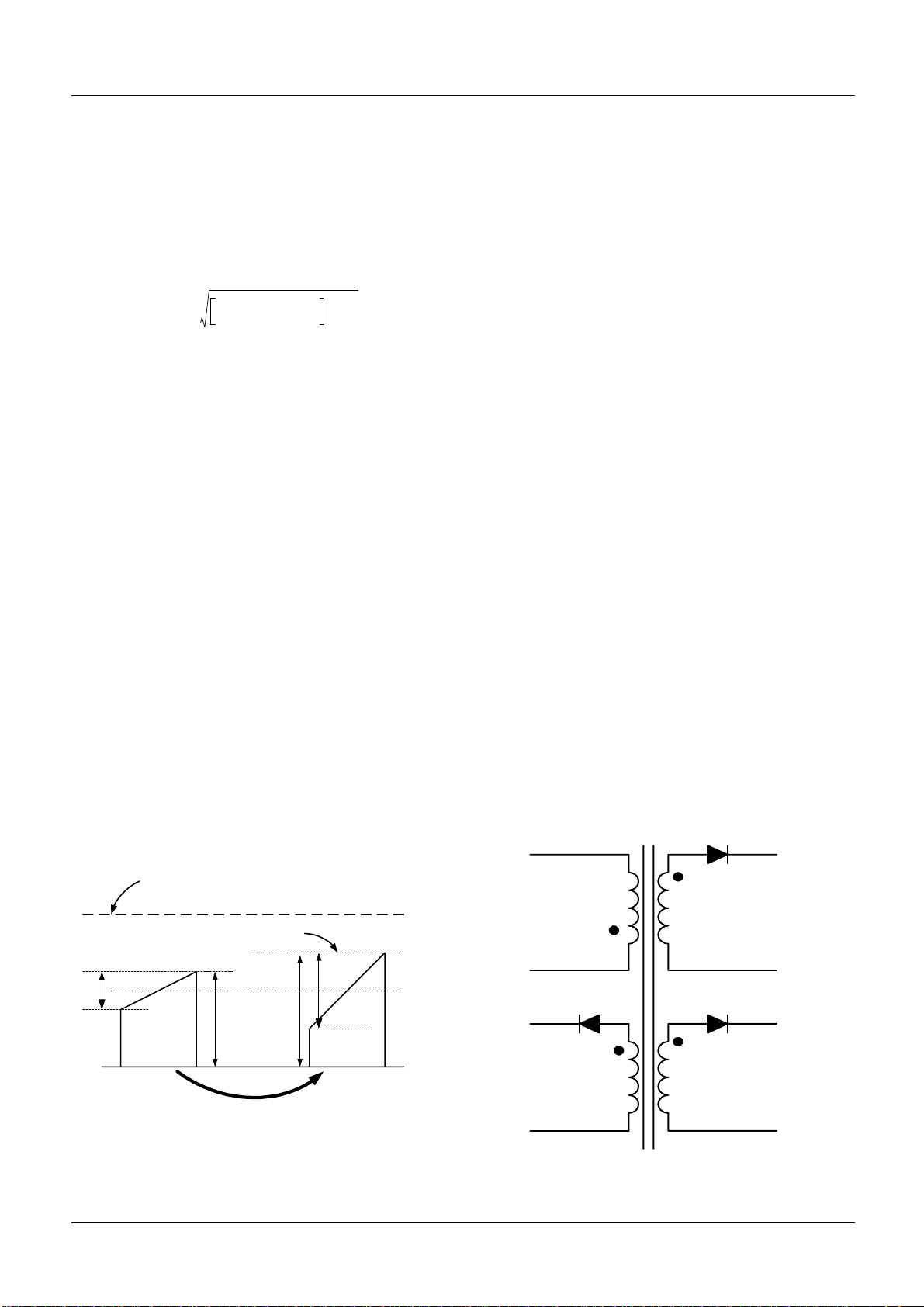
(b) Vcc winding
is
m
In general, the voltage of each winding is influenced by the
voltage of the adjacent winding. The optimum placement of
the Vcc winding is determined by the over voltage pro tection
(OVP) sensitivity, the Vcc operating range and control
scheme.
-Over voltage protection (OVP) sensitivity : When the
2
output voltage goes above its normal operation value due to
some abnormal situation, Vcc voltage also increases. FPS
2
uses Vcc voltage to indirectly monitor the over voltage
is
situation in the secondary side. However, a RCD snubber
network acts as an another output as shown in Figure 8 and
Vcc voltage is also influenced by the snubber capacitor
voltage. Because the snubber voltage increases as the drain
current increases, OVP of FPS can be triggered not only by
the output over voltage condition, but also by the over load
condition.
The sensitivity of over voltage protection is closely related to
the physical distance between windings. If the Vcc winding
is close to the secondary side output winding, Vcc voltage
will change sensitively to the variation of th e output voltage.
Meanwhile, if the Vcc winding is placed close to the primar y
side winding, Vcc voltage will vary sensitively as the
snubber capacitor voltage changes.
(a) Primary winding
3mm 3mm
Barrier tape
Insulation tape
...... Na ...
.......... Ns .........
....... Np/2 .....
........ Np/2 ..... .
Bobbin
To FPS Drain pin
Figure 7. Primary side winding
It is typical to place all the primary winding or a portion of
the primary winding innermost on the bobbin. This
minimizes the length of wire, reducing the conduction loss in
the wire. The EMI noise radiation can be reduced, since the
-
V
sn
+
Np
+
V
cc
N
a
-
Figure 8. Primary side winding
N
S2
N
S1
+
V
O2
-
+
V
O1
-
4
©2002 Fairchild Semiconductor Corporation

APPLICATION NOTE AN4140
- Vcc operating range : As menti one d ab ove, Vcc voltage is
influenced by the snubber capacitor voltage. Since the
snubber capacitor voltage changes according to drain
current, Vcc voltage can go above its operating range
Secondary winding
(4 turns)
triggering OVP in normal operation. In that case, Vcc
winding should be placed closest to the reference output
winding that is regulated by feedback control and far from
the primary side winding as shown in Figure 9.
3mm 3mm
...... Na (Vcc winding) .....
..... Ns1 (Reference output) .....
........ Ns2 .......
Figure 10. Multiple parallel strands winding
.......... Np .........
.............. Np ..............
Secondary winding
(3 strands, 4 turns)
.............. Np ..............
Figure 9. Winding sequence to reduce Vcc variation
- Control scheme : In the case of primary side regulation,
the output voltages should follow the Vcc voltage tightly for
a good output regulation. Therefore, Vcc winding should be
placed close to the secondary windings to maximize the
coupling of the Vcc winding with the secondary windings.
Meanwhile, Vcc winding should be placed far from primary
winding to minimize coupling to the primary. In the case of
secondary side regulation, the Vcc winding can be placed
between the primary and secondary or on the outermost
position.
(c) Secondary side winding
When it comes to a transform er with multiple outputs, the
highest output power winding should be placed clos est to the
primary side winding, to reduce leakage inductance and to
maximize energy transfer efficiency. If a secondary side
winding has relatively few turns, the winding should be
spaced to traverse the entire width of the winding area for
improved cou pling. Using multipl e parallel strands of wi re
will also help to increase the fill factor and couplin g for the
secondary wi ndings with few t urns as shown in Figu re 10.
To maximize the load regulation, the winding of the output
with tight regulation requirement should be placed closest to
the winding of the reference output that is regulated by the
feedback control.
(2) Winding method
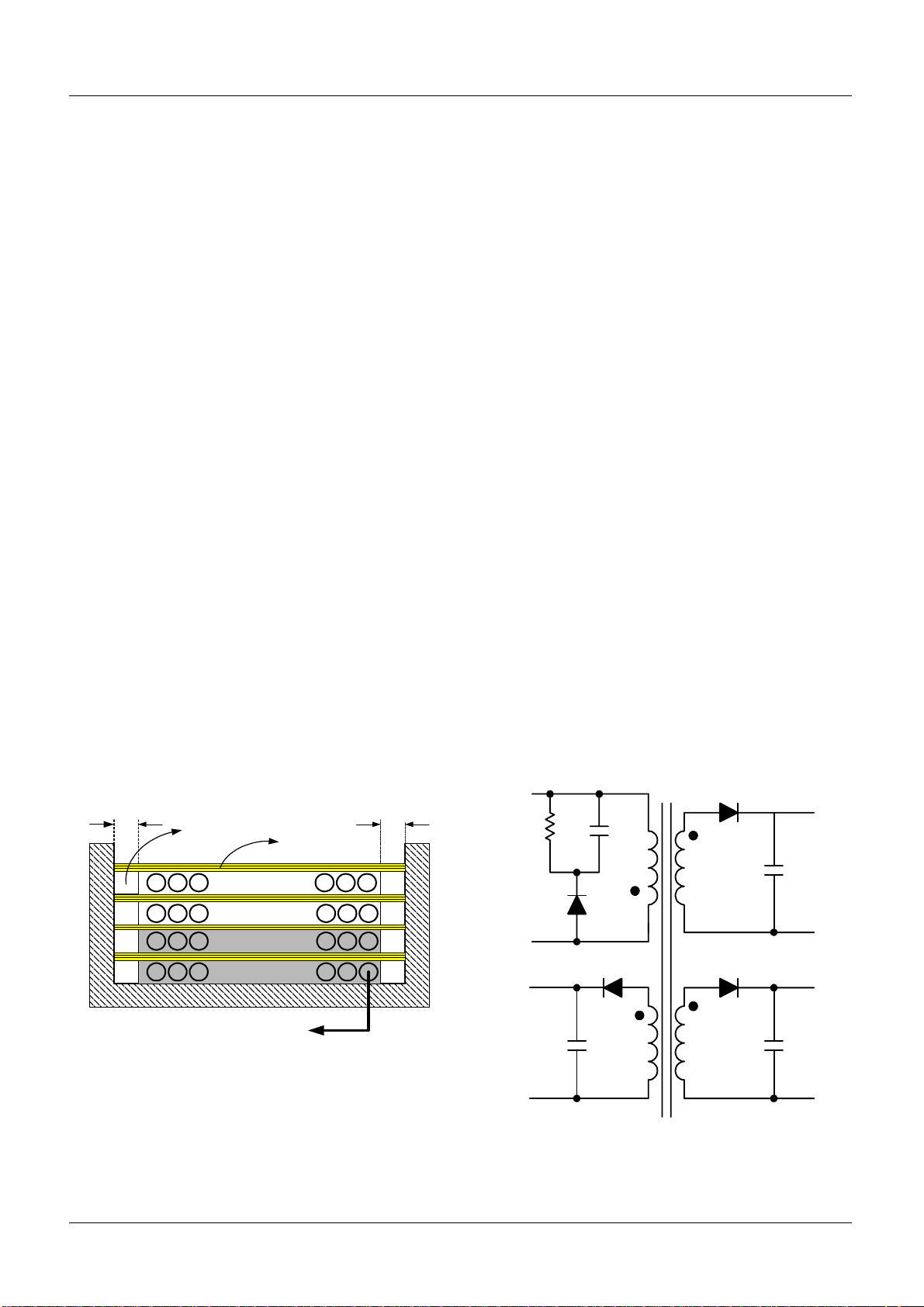
-Stacked winding on other winding: A common technique
for winding multiple outputs with the same polarity sharing a
common ground is to stack the secondary windings instead
of winding each output winding separately, as shown in
Figure 11. This approach will improve the load regulation of
the stacked outputs and reduce the total number of secondary
turns. The windings for the lowest voltage output provide the
return and part of the winding turns for the next higher
voltage output. The turns of both the lowest output and the
next higher output provide turns for succeeding outputs. The
wire for each output must be sized to accommodate its
output current plus the sum of the output currents of all the
output stacked on top of it.
-Stacked winding on other output: If a transformer has a
very high voltage and lo w curr ent ou tput, the winding can be
stacked on the lower voltage output as shown in Figure 12.
This approach provides better regulation and reduced diode
voltage stress for the stacked output. The wire and rectifier
diode for each output must be sized to accommodate its
output current plus the sum of the output currents of all the
output stacked on top of it.
©2002 Fairchild Semiconductor Corporation
5

AN4140 APPLICATION NOTE
the leakage inductance is a sandwich winding as shown in
D
R2
Figure 13. Se co nda ry w in din gs w i th onl y a fe w t ur ns shou ld
be spaced across the width of the bobbin window instead of
being bunched together, in order to maximize coupling to the
Np
N
S2
D
R1
N
S1
V
O2
V
O1
primary. Using multiple parallel strands of wire is an
additional technique of increasing the fill factor and coupling
of a winding with few turns as shown in Figure 10.
3mm 3mm
.............. Na ..............
.............. Np/2 ..............
.............. Ns1 ..............
Figure 11. Stacked winding on other winding
D
R2
V
Np
N
S2
O2
(4)
Transformer shielding
.............. Ns2 ..............
.............. Np/2 ..............
Figure 13. Sandwich winding
A major source of common mode EMI in Switched Mode
Power Supply (SMPS) is the parasi tic capacitances coupled
D
R1
to the switching devices. The MOSFET drain voltage drives
capacitive current through various parasitic capacitances.
V
O1
N
S1
Some portion of these capacitive currents flow into the
neutral line that is connected to the earth ground and
observed as common mode noise. By using an electrostatic
separation shield between the windings (at primary winding
side, or at secondary winding side, or both), the common
mode signal is effectively "shorted" to the ground and the
capacitive current is reduced. When properly designed, such
shielding can dramatically reduce the conducted and radiated
emissions and susceptibility. By using this technique, the
Figure 12. Stacked winding on other output
size of EMI filter can be reduced. The shield can be easily
implemented using copper foil or tightly wound wire. The
shield should be virtually grounded to a quiescent point s uch
as primary side DC link, primary ground or secondary
ground.
(3)
Minimization of Leakage Inductance
The winding order in a transformer has a large effect on the
leakage inductance. In a multiple output transformer, the
secondary with the highest output power should be placed
closest to the primary for the best coupling and lowest
leakage. The most common and effective way to minimize
6
Figure 14 shows a shielding example, which allows the
removal of the Y-capacitor that is commonly used to reduce
common mode EMI. As can be seen, shields are used not
only on the bottom but also on the top of the primary
winding in order to cancel the coupling of parasitic capaci-
tances. Figure 15 also shows the detailed shielding
construction.
©2002 Fairchild Semiconductor Corporation

AN4140 APPLICATION NOTE
DC link
TOP
Insulation Tape Copper Foil
Np
N
S
Shielding A
Drain
BOTTOM
Shielding B
#1 #2 #3 #4 #5
N
a
Winding Direction
3mm 3mm
.............. Na ..............
.............. Ns ............. .
Shield B
Insulation Tape
.............. Np ..............
#1 #2 #3 #4 #5
Primary Winding
Winding Directio
Copper Foil
Shield A
Figure 14. Shielding example to remove Y-capacitor
(5) Practical examples of transformer
construction
As described in the above sections, there many factors that
should be considered in determining the winding sequence
and winding method. In this section some practical examples
of transformer construction are presented to give a comprehensive understanding of practical transformer construction.
#1 #2 #3 #4 #5
Figure 15. Shielding method to remove Y-Capacitor
a) LCD monitor SMPS example
Figure 16 shows a simplified transformer schematic for
typical LCD monitor SMPS. The 5V output is for the Microprocessor and 13V output is for the inverter input of LCD
back light. While 5V output is regulated with the feedback
control, 13V output is determined by the transformer tu rns
ratio and a stacked winding is usually used to maximize the
regulation.
7
©2003 Fairchild Semiconductor Corporation

APPLICATION NOTE AN4140
Transformer construction Example A (Figure 17) : In this
example, the leakage inductance is minimized by employing
a sandwich winding. The Vcc winding is placed outside to
3mm 3mm
provide shielding effect. Since the Vcc winding is placed on
the top half of primary winding, the coupl ing between the
Vcc winding and 5V output winding is poor, which may
require a small dummy load on the 5V output to prevent
UVLO (Under Voltage Lock Out) in the no load condition.
Transformer construction Example B (Figure 18)
: In this
Na
example, the leakage inductance is larger than example A,
since a sandwich winding is not used. However, the Vcc
winding is tightly coupled with the 5V output winding and
Vcc remains its normal operation range in the no load
condition. Even though this approach can prevent U VLO in
no load conditions without dummy load, the power
Ns1
Ns2
Np
conversion efficiency might be relatively poor compared to
example A due to the large leakage inductance.
Figure 18. LCD monitor SMPS transformer construction
D
R2
example (B)
Np
N
S2
V
O2
(13V/2.5A)
D
R1
V
N
cc
a
N
S1
V
O1
(5V/2A)
Figure 16. LCD monitor SMPS transformer example
3mm 3mm
Na
Np/2
Ns1
(b) CRT monitor SMPS ex ample - PSR ( Primar y side
regulation)
Figure 19 shows a simplified transformer schematic for a
typical CRT monitor SMPS employing PSR (Primary side
regulation). 80V and 50V outp ut s ar e the mai n o utpu t having
high output power. Meanwhile, 5V and 6.5V outputs are
auxiliary outp ut h avi ng smal l ou tput pow er. The 80 V ou tput
winding is stacked on the 50V output to reduce the voltage
stress of the rectifier diode (D
D
R1
N
S1
D
R2
N
Np
N
a
S2
D
R3
N
S3
R1
7805
7805
78057805
V
O3
(14V)
).
V
O1
(80V)
(50V)
5V
V
O2
Main output
with large
power
Ns2
Np/2
Figure 17. LCD monitor SMPS transformer construction
example (A)
©2003 Fairchild Semiconductor Corporation
D
R4
V
O4
N
S4
(6.5V)
Aux output
with small
power
Figure 19. CRT monitor SMPS transformer example-PSR
8

APPLICATION NOTE AN4140
Figure 20 shows the detailed transformer construction. In
order to minimize the leakage inductance, sandwich winding
is employed and the main output windings are placed closest
to the primary winding. The Vcc winding is placed closest to
the main output windings to provide tig ht regulations of the
main output. The auxiliary output windings are placed
outside of the primary winding to provide a shielding effect.
3mm 3mm
Ns4
Ns3
Np/2
Ns1
Na
Ns1
Np/2
D
R1
Main output
with large
power
V
N
S1
O1
(80V)
Reference
7805
7805
78057805
O3
output
V
(50V)
5V
V
O4
(6.5V )
O2
D
R2
N
S2
Np
D
R3
N
N
V
cc
a
S3
D
R4
N
S4
V
(14V)
Aux output
with small
power
Figure 20. CRT monitor SMPS transformer construction
example (PSR)
(c) CRT monitor SMPS example - SSR (Secondary
side regulation)
Figure 21 shows a simplified transformer schematic for
typical CRT monitor SMPS employing SSR (Secondary side
regulation). 80V and 50V outputs are the main output having
high output power. Meanwhile, 5V and 6.5V outputs are
auxiliary output having small output power. The 80V output
winding is stacked o n 50V ou tput to reduce t he volt age stres s
of the rectifier diode (D
R1
).
Figure 22 shows the detailed transformer construction. In
order to minimize the leakage inductance, a sandwich
winding is employed and the main output windings are
placed closest to the primary winding. The Vcc winding is
placed outermost to provide a shielding effect. The auxiliary
output windings are placed between windings of the main
output winding to obtain bett er regulation.
Figure 21. CRT monitor SMPS transformer example-SSR
3mm 3mm
Na
Np/2
Ns2
Ns4
Ns3
Ns1
Np/2
Figure 22. CRT monitor SMPS transformer construction
example (SSR)
©2002 Fairchild Semiconductor Corporation
9

AN4140 APPLICATION NOTE
References
Colonel Wm. T. McLyman, Transformer and Inductor
design Handbook, 2nd ed. Marcel Dekker, 1988.
Anatoly Tsaliovich, Electromagnetic shielding handbook for
wired and wireless EMC application, 1998
Bruce C. Gabrielson and Mark J. Reimold, "Suppression of
Powerline noise with isolation transformers", EMC expo87
San Diego, 1987.
D.Cochrane, D.Y.Chen, D. Boroyevich, "Passive cancellation of common mode noise in power electronics circuits,"
PESC 2001, pp.1025-1029
Otakar A. Horna, "HF Transformer with triaxial cable
shielding against capacitive current", IEEE Transactions on
parts, hybrids, and packaging, vol.php-7, N0.3 , Sep. 1971.
10
©2002 Fairchild Semiconductor Corporation

AN4140 APPLICATION NOTE
by Hang-Seok Choi / Ph. D
Power Supply Group / Fairchild Semiconductor
Phone : +82-32-680-1383 Facsimile : +82-32-680-1317
E-mail : hschoi@fairchildsemi.co.kr
DISCLAIMER
FAIRCHILD SEMICONDUCTOR RESERVES THE RIGHT TO MAKE CHANGES WITHOUT FURTHER NOTICE TO ANY
PRODUCTS HEREIN TO IMPROVE RELIABILITY, FUNCTION OR DESIGN. FAIRCHILD DOES NOT ASSUME ANY
LIABILITY ARISING OUT OF THE APPLICATION OR USE OF ANY PRODUCT OR CIRCUIT DESCRIBED HEREIN; NEITHER
DOES IT CONVEY ANY LICENSE UNDER ITS PATENT RIGHTS, NOR THE RIGHTS OF OTHERS.
LIFE SUPPORT POLICY
FAIRCHILD’S PRODUCTS ARE NOT AUTHORIZED FOR USE AS CRITICAL COMPONENTS IN LIFE SUPPORT DEVICES
OR SYSTEMS WITHOUT THE EXPRESS WRITTEN APPROVAL OF THE PRESIDENT OF FAIRCHILD SEMICONDUCTOR
CORPROATION. As used herein:
1. Life support devices or systems are devices or systems
which, (a) are intended for surgical implant into the body,
or (b) support or sustain lif e, or (c) whose failure to perfo rm
when properly used in a ccordance with instructions for us e
provided in the labeling, can be reasonably expected to
result in significant injury to the user.
2. A critical component is any component of a life support
device or system whose failure to perform can be
reasonably expected to cause the failure of t he life support
device or system, or to affect its safety or effectiveness.
www.fairchildsemi.com
2003 Fairchild Semiconductor Corporation
3/24/04 0.0m 002
 Loading...