

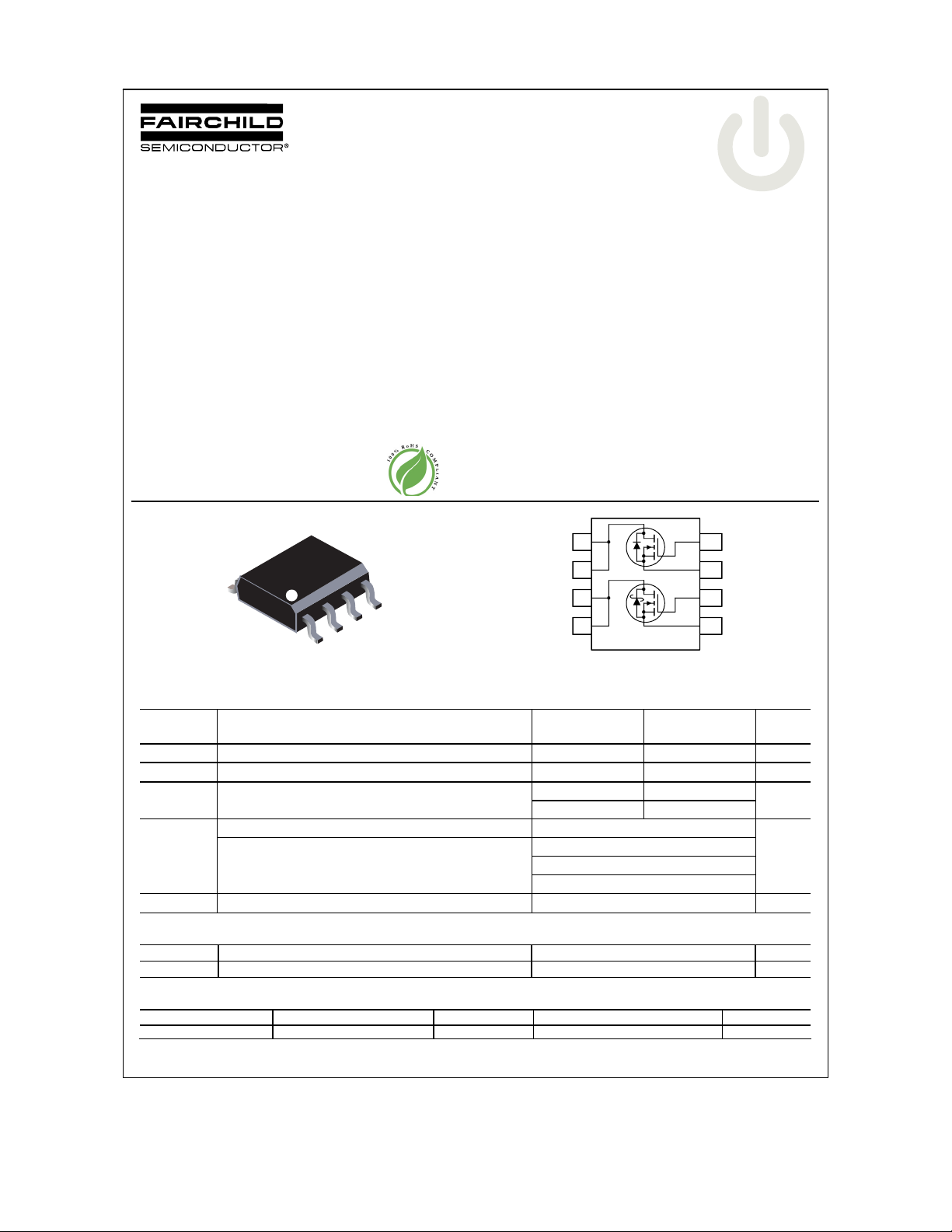
FDS6982AS
May 2008
FDS6982AS
Dual Notebook Power Supply N-Channel PowerTrench® SyncFET™
General Description
The FDS6982AS is designed to replace two single SO8 MOSFETs and Schottky diode in synchronous
DC:DC power supplies that provide various peripheral
voltages for notebook computers and other battery
powered electronic devices. FDS6982AS contains two
unique 30V, N-channel, logic level, PowerTrench
MOSFETs designed to maximize power conversion
efficiency. The high-side switch (Q1) is designed with
specific emphasis on reducing switching losses while
the low-side switch (Q2) is optimized to reduce
conduction losses. Q2 also includes an integrated
Schottky diode using Fairchild’s monolithic SyncFET
technology.
Applications
• Notebook
D1
D1
D2
D2
G1
S2
G2
S1
= 25°C unless otherwise noted
A
SO-8
Absolute Maximum Ratings T
Features
• Q2: Optimized to minimize conduction losses
Includes SyncFET Schottky body diode
8.6A, 30V R
R
• Low gate charge (21nC typical)
• Q1: Optimized for low switching losses
6.3A, 30V R
R
• Low gate charge (11nC typical)
5
6
7
8
max= 13.5mΩ @ VGS = 10V
DS(on)
max= 16.5mΩ @ VGS = 4.5V
DS(on)
max= 28.0mΩ @ V
DS(on)
max= 35.0mΩ @ V
DS(on)
4
Q1
Q2
3
2
1
tmM
= 10V
GS
= 4.5V
GS
Symbol Parameter Q2 Q1 Units
V
Drain-Source Voltage 30 30 V
DSS
V
Gate-Source Voltage
GSS
ID Drain Current - Continuous (Note 1a) 8.6 6.3 A
- Pulsed 30 20
PD Power Dissipation for Dual Operation 2 W
Power Dissipation for Single Operation (Note 1a) 1.6
TJ, T
STG
Operating and Storage Junction Temperature Range –55 to +150
(Note 1b)
(Note 1c)
±20 ±20
1
0.9
V
°C
Thermal Characteristics
R
θJA
R
θJC
Thermal Resistance, Junction-to-Ambient
Thermal Resistance, Junction-to-Case
(Note 1a) 78
(Note 1) 40
°C/W
°C/W
Package Marking and Ordering Information
Device Marking Device Reel Size Tape width Quantity
FDS6982AS FDS6982AS 13” 12mm 2500 units
©2008 Fairchild Semiconductor Corpora tion
FDS6982AS Rev B1
FDS6982AS
Electrical Characteristics T
= 25°C unless otherwise noted
A
Symbol Parameter Test Conditions Type Min Typ Max Units
Off Characteristics
BV
Drain-Source Breakdown
DSS
Voltage
∆BVDSS
∆T
I
DSS
Breakdown Voltage
Temperature Coefficient
J
Zero Gate Voltage Drain
Current
I
Gate-Body Leakage
GSS
VGS = 0 V, ID = 1 mA
= 0 V, ID = 250 uA
V
GS
I
= 1 mA, Referenced to 25°C
D
= 250 µA, Referenced to 25°C
I
D
Q1
Q2
Q1
VDS = 24 V, VGS = 0 V Q2
Q1
V
= ±20 V, VDS = 0 V
GS
Q2
Q1
30
30
V
28
24
mV/°C
500
1
±100
Q2
On Characteristics (Note 2)
V
Gate Threshold Voltage VDS = VGS, ID = 1 mA
GS(th)
∆VGS(th)
∆TJ
R
DS(on)
Gate Threshold Voltage
Temperature Coefficient
Static Drain-Source
On-Resistance
I
On-State Drain Current VGS = 10 V, VDS = 5 V Q2
D(on)
V
= VGS, ID = 250 µA
DS
ID = 1 mA, Referenced to 25°C
I
= 250 uA, Referenced to 25°C
D
VGS = 10 V, ID = 8.6 A
= 10 V, ID = 8.6 A, TJ = 125°C
V
GS
V
= 4.5 V, ID = 7.5 A
GS
V
= 10 V, ID = 6.3 A
GS
= 10 V, ID = 6.3 A, TJ = 125°C
V
GS
= 4.5 V, ID = 5.6 A
V
GS
gFS Forward Transconductance VDS = 5 V, ID = 8.6 A
= 5 V, ID = 6.3 A
V
DS
Q2
Q1 1 1
1.4
1.9 3 3
Q2 –3.1
Q1 –4.3
Q2
11
Q1 20
30
Q1
Q2
20
32
Q1
13.5
20.0
16
16.5
13
28
26
33
25
35
A
S
19
mV/°C
mΩ
Dynamic Characteristics
C
Input Capacitance Q2
iss
C
Output Capacitance Q2
oss
C
Reverse Transfer Capacitance
rss
RG Gate Resistance VGS = 15mV, f = 1.0 MHz Q2
V
= 10 V, VGS = 0 V,
DS
f = 1.0 MHz
Q1
Q1
Q2
Q1
Q1
1250
610
410
180
130
85
1.4
2.2
pF
pF
pF
Switching Characteristics (Note 2)
t
Turn-On Delay Time
d(on)
tr Turn-On Rise Time
t
Turn-Off Delay Time
d(off)
tf Turn-Off Fall Time
t
Turn-On Delay Time
d(on)
tr Turn-On Rise Time
t
Turn-Off Delay Time
d(off)
tf Turn-Off Fall Time
= 15 V, ID = 1 A,
V
DD
= 10V, R
V
GS
V
= 15 V, ID = 1 A,
DD
= 4.5V, R
V
GS
GEN
GEN
= 6 Ω
= 6 Ω
Q2
Q1
Q2
Q1
Q2
Q1
Q2
Q1
Q2
Q1
Q2
Q1
Q2
Q1
Q2
Q1
9
10
18
20
6 7 12
14
27
24
44
39
11 3 20 6 ns
12
13
19
12
14
15
22
22
23
25
34
27
10 5 20
10
µA
nA
V
Ω
ns
ns
ns
ns
ns
ns
ns
FDS6982AS Rev B1
FDS6982AS
Electrical Characteristics (continued) T
Symbol
Parameter
Test Conditions
= 25°C unless otherwise noted
A
Type Min Typ Max Units
Switching Characteristics (Note 2)
Q
Qg
Qgs
Qgd
g
(TOT)
Total Gate Charge at Vgs=10V
Total Gate Charge at Vgs=5V
Gate–Source Charge
Gate–Drain Charge
Q2:
V
= 15 V, ID = 11.5A
DS
Q1:
V
= 15 V, ID = 6.3A
DS
Q2
Q1
Q2
Q1
Q2
Q1
Q2
Q1
21
11
12 6 16 9 nC
3.1
1.8
3.6
2.4
Drain–Source Diode Characteristics and Maximum Ratings
IS Maximum Continuous Drain-Source Diode Forward Current Q2
Q1
Trr Reverse Recovery Time
Qrr Reverse Recovery Charge
Trr Reverse Recovery Time
Qrr Reverse Recovery Charge
VSD Drain-Source Diode Forward
Voltage
I
= 11.5 A,
F
d
= 300 A/µs (Note 3)
iF/dt
I
= 6.3 A,
F
d
= 100 A/µs (Note 3)
iF/dt
VGS = 0 V, IS = 3 A (Note 2)
VGS = 0 V, IS = 6 A (Note 2)
VGS = 0 V, IS = 1.3 A (Note 2)
Notes:
1. R
is the sum of the junction-to-case and case-to-ambient thermal resistance where the case thermal reference is defined as the solder mounting surface of
θJA
the drain pins. R
is guaranteed by design while R
θJC
is determined by the user's board design.
θCA
Q2
Q1
Q2
Q2
Q1
3.0
19
12 nC
20
9 nC
0.5
0.6
0.8
30
nC
15
nC
nC
A
1.3
ns
ns
0.7
1.0
V
1.2
a) 78°C/W when
mounted on a
0.5in2 pad of 2
oz copper
Scale 1 : 1 on letter size paper
2. Pulse Test: Pulse Width < 300µs, Duty Cycle < 2.0%
3. See “SyncFET Schottky body diode characteristics” below.
4
5
b) 125°C/W when
mounted on a
0.02 in2 pad of
2 oz copper
c) 135°C/W when
mounted on a
minimum pad.
FDS6982AS Rev B1

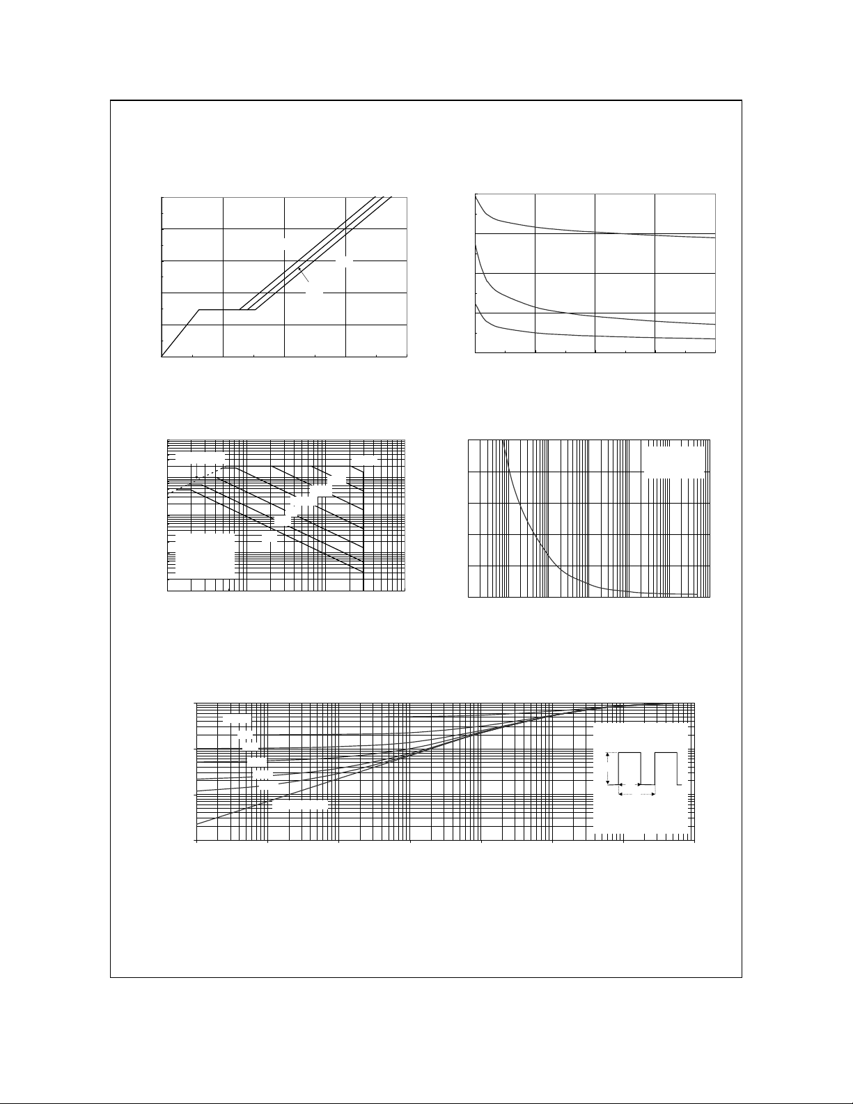
Typical Characteristics: Q2
FDS6982AS
30
VGS = 10V
20
10
, DRAIN CURRENT (A)
D
I
0
00.511.52
4.5V
V
, DRAIN-SOURCE VOLTAGE (V )
DS
3.0V
3.5V
2.5V
2.6
VGS = 2.5V
2.4
2.2
2
1.8
, NORMALIZED
R
1.6
1.4
DS(ON)
1.2
1
DRAIN-SOURCE ON-RESISTANCE
0.8
3.0V
3.5V
4.0V
4.5V
6.0V
0 102030
, DRAIN CURRENT (A)
I
D
Figure 1. On-Region Characteristics. Figure 2. On-Resistance Variation with
Drain Current and Gate Voltage.
1.4
ID = 8.6A
V
= 10V
GS
1.2
1
, NORMALIZED
DS(ON)
R
0.8
DRAIN-SOURCE ON-RESISTANCE
0.6
-50-250 255075100125
, JUNCTION TEMPERATURE (oC)
T
J
Figure 3. On-Resistance Variation with
Temperature.
0.05
0.04
0.03
TA = 125oC
0.02
, ON-RESISTANCE (OHM)
0.01
DS(ON)
R
TA = 25oC
0
246810
, GATE TO SOURCE VOLTAGE (V)
V
GS
Figure 4. On-Resistance Variation with
Gate-to-Source Voltage.
10V
ID = 4.3 A
30
VDS = 5V
25
20
15
10
, DRAIN CURRENT (A)
D
I
5
0
11.522.533.5
V
TA = 125oC
-55oC
25oC
, GATE TO SOURCE VOLTAGE (V)
GS
Figure 5. Transfer Characteristics. Figure 6. Body Diode Forward Voltage Variation
10
VGS = 0V
1
TA = 125oC
25oC
0.1
, REVERSE DRAIN CURRENT (A)
S
I
0.01
0 0.2 0.4 0.6 0.8
V
, BODY DIODE FORWARD VOLTAGE (V)
SD
-55oC
with Source Current and Temperature.
FDS6982AS Rev B1

Typical Characteristics: Q2
FDS6982AS
10
ID = 8.6A
8
6
4
, GATE-SOURCE VOLTAGE (V)
2
GS
V
0
0 5 10 15 20 25
VDS = 10V
, GATE CHARGE (nC)
Q
g
20V
15V
2000
1600
1200
800
C
CAPACITANCE (pF)
400
C
rss
0
0 5 10 15 20 25 30
oss
V
, DRAIN TO SOURCE VOLTAGE (V)
DS
C
iss
Figure 7. Gate Charge Characteristics. Figure 8. Capacitance Characteristics.
100
R
LIMIT
DS(ON)
10
100ms
1s
1
, DRAIN CURRENT (A)
D
I
VGS = 10V
SINGLE PULSE
0.1
0.01
= 135oC/W
R
θ
JA
= 25oC
T
A
0.1 1 10 100
V
DS
10s
DC
, DRAIN-SOURCE VOLTAGE (V)
10ms
100µs
1ms
50
40
30
20
10
P(pk), PEAK TRANSIENT POWER (W)
0
0.001 0.01 0.1 1 10 100 1000
, TIME (sec)
t
1
SINGLE PULSE
R
Figure 9. Maximum Safe Operating Area. Figure 10. Single Pulse Maximum
Power Dissipation.
= 135°C/W
JA
θ
= 25°C
T
A
f = 1MHz
V
= 0 V
GS
1
D = 0.5
0.2
0.1
0.01
0.1
0.05
0.02
0.01
SINGLE PULSE
r(t), NORMALIZED EFFECTIVE
TRANSIENT THERMAL RESISTANCE
0.001
R
(t) = r(t) * R
JA
θ
R
= 135°C/W
JA
θ
P(pk)
t
1
t
2
- TA = P * R
T
J
Duty Cycle, D = t
JA
θ
(t)
JA
θ
/ t
1
2
0.0001 0.001 0.01 0.1 1 10 100 1000
t
, TIME (sec)
1
Figure 11. Transient Thermal Response Curve.
Thermal characterization performed using the conditions described in Note 1c.
Transient thermal response will change depending on the circuit board design.
FDS6982AS Rev B1

Typical Characteristics Q1
FDS6982AS
20
VGS = 10V
16
12
, DRAIN CURRENT (A)
D
I
6.0V
8
4
0
012
4.0V
4.5V
, DRAIN-SOURCE VOLTA GE (V )
V
DS
3.5V
3.0V
2.6
VGS = 3.0V
2.2
1.8
, NORMALIZED
1.4
DS(ON)
R
1
DRAIN-SOURCE ON-RESISTANCE
0.6
3.5V
4.0V
4.5V
6.0V
0 5 10 15 20
I
, DRAIN CURRENT (A)
D
Figure 12. On-Region Characteristics. Figure 13. On-Resistance Variation with
Drain Current and Gate Voltage.
1.6
ID = 6.3A
= 10V
V
GS
1.4
1.2
, NORMALIZED
1
DS(ON)
R
0.8
DRAIN-SOURCE ON-RESISTANCE
0.6
-50 -25 0 25 50 75 100 125 150
T
, JUNCTION TEMPERATURE (oC)
J
Figure 14. On-Resistance Variation with
Temperature.
0.1
0.08
0.06
0.04
, ON-RESISTANCE (OHM)
0.02
DS(ON)
R
TA = 25oC
0
246810
V
TA = 125oC
, GATE TO SOURCE VOLTAGE (V)
GS
Figure 15. On-Resistance Variation with
Gate-to-Source Voltage.
10V
ID = 3.15 A
20
VDS = 5V
15
10
, DRAIN CURRENT (A)
D
5
I
0
11.522.533.5
V
, GATE TO SOURCE VOLTAGE (V)
GS
TA = 125oC
-55oC
25oC
100
VGS = 0V
10
1
0.1
0.01
0.001
, REVERSE DRAIN CURRENT (A)
S
I
0.0001
0 0.2 0.4 0.6 0.8 1 1.2 1.4
TA = 125oC
25oC
-55oC
, BODY DIODE FORWARD VOLTAGE (V)
V
SD
Figure 16. Transfer Characteristics. Figure 17. Body Diode Forward Voltage Variation
with Source Current and Temperature.
FDS6982AS Rev B1
Typical Characteristics Q1
FDS6982AS
10
ID = 6.3A
8
VDS = 10V
6
4
, GATE-SOURCE VOLTAGE (V)
2
GS
V
0
036912
, GATE CHARGE (nC)
Q
g
20V
15V
800
600
C
iss
400
C
CAPACITANCE (pF)
200
C
rss
0
0 5 10 15 20
V
oss
, DRAIN TO SOURCE VOLTAGE (V)
DS
Figure 18. Gate Charge Characteristics. Figure 19. Capacitance Characteristics.
100
R
LIMIT
DS(ON)
10
1
VGS = 10V
SINGLE PULSE
, DRAIN CURRENT (A)
0.1
D
I
0.01
= 135oC/W
R
JA
θ
T
= 25oC
A
0.1 1 10 100
DC
, DRAIN-SOURCE VOLTAGE (V)
V
DS
10s
100ms
1s
10ms
100µs
1ms
50
40
30
20
10
P(pk), PEAK TRANSIENT POWER (W)
0
0.001 0.01 0.1 1 10 100 1000
, TIME (sec)
t
1
SINGLE PULSE
R
JA
θ
T
Figure 20. Maximum Safe Operating Area. Figure 21. Single Pulse Maximum
Power Dissipation.
f = 1MHz
= 0 V
V
GS
= 135°C/W
= 25°C
A
1
D = 0.5
0.2
0.1
0.01
r(t), NORMALIZED EFFECTIVE
TRANSIENT THERMAL RESISTANCE
0.001
0.1
0.05
0.02
0.01
SINGLE PULSE
0.0001 0.001 0.01 0.1 1 10 100 1000
, TIME (sec)
t
1
Figure 22. Transient Thermal Response Curve.
Thermal characterization performed using the conditions described in Note 1c.
Transient thermal response will change depending on the circuit board design.
R
JA
θ
R
θ
P(pk)
T
- TA = P * R
J
Duty Cycle, D = t
(t) = r(t) * R
= 135°C/W
JA
t
1
t
2
JA
θ
(t)
JA
θ
/ t
1
2
FDS6982AS Rev B1

Typical Characteristics (continued)
SyncFET Schottky Body Diode
Characteristics
FDS6982AS
Fairchild’s SyncFET process embeds a Schottky diode
in parallel with PowerTrench MOSFET. This diode
exhibits similar characteristics to a discrete external
Schottky diode in parallel with a MOSFET. Figure 23
shows the reverse recovery characteristic of the
FDS6982AS.
Current: 1.6A/DIV
Time: 10nS/DIV
Figure 23. FDS6982AS SyncFET body
diode reverse recovery characteristic.
For comparison purposes, Figure 24 shows the reverse
recovery characteristics of the body diode of an
equivalent size MOSFET produced without SyncFET
(FDS6982).
Current: 1.6A/DIV
Time: 10nS/DIV
Figure 24. Non-SyncFET (FDS6982) body
diode reverse recovery characteristic.
Schottky barrier diodes exhibit significant leakage at
high temperature and high reverse voltage. This will
increase the power in the device.
0.1
0.01
0.001
0.0001
0.00001
, REVERSE LEAKAGE CURRENT (A)
DSS
I
0.000001
0 5 10 15 20 25 30
TA = 125oC
TA = 100oC
TA = 25oC
, REVERSE VOLTAGE (V)
V
DS
Figure 25. SyncFET body diode reverse
leakage versus drain-source voltage and
temperature
FDS6982AS Rev B1

Typical Characteristics
FDS6982AS
I
AS
L
DUT
0.01Ω
+
V
-
V
V
GS
R
GE
0V
V
GS
vary tP to obtain
required peak I
DS
tp
AS
Figure 26. Unclamped Inductive Load Test
Circuit
Drain Current
Same type as
+
10V
-
10µF
50kΩ
1µF
+
V
-
V
GS
DUT
I
g(REF
BV
t
P
I
DD
AS
Figure 27. Unclamped Inductive
Waveforms
DD
Q
G(TOT)
10V
GS
Q
GD
V
GS
Q
t
AV
DSS
V
DS
V
DD
Charge, (nC)
Figure 28. Gate Charge Test Circuit Figure 29. Gate Charge Waveform
t
R
L
DUT
V
R
GEN
V
GS
Pulse Width ≤ 1µs
Duty Cycle ≤ 0.1%
V
GS
DS
Figure 30. Switching Time Test
ON
t
d(ON)
V
DS
+
V
DD
0V
90%
10%
t
r
-
V
GS
0V
10%
50%
Pulse Width
Figure 31. Switching Time Waveforms
t
d(OFF
)
90%
t
50%
OFF
t
10%
f
90%
Circuit
FDS6982AS Rev B1

TRADEMARKS
®
tm
tm
The following includes registered and unregistered trademarks and service marks, owned by Fairchild Semiconductor and/or its global
subsidianries, and is not intended to be an exhaustive list of all such trademarks.
®
ACEx
Build it Now™
CorePLUS™
CorePOWER™
CROSSVOLT™
CTL™
Current Transfer Logic™
EcoSPARK
®
EfficentMax™
EZSWITCH™ *
™
Fairchild
Fairchild Semiconductor
FACT Quiet Series™
FACT
FAST
FastvCore™
FlashWriter
®
®
®
®
®
*
* EZSWITCH™ and FlashWriter
FPS™
F-PFS™
®
FRFET
Global Power Resource
Green FPS™
Green FPS™ e-Series™
GTO™
IntelliMAX™
ISOPLANAR™
MegaBuck™
MICROCOUPLER™
MicroFET™
MicroPak™
MillerDrive™
MotionMax™
Motion-SPM™
OPTOLOGIC
OPTOPLANAR
®
®
are trademarks of System General Corporation, used under license by Fairchild Semiconductor.
®
®
PDP-SPM™
Power-SPM™
PowerTrench
SM
Programmable Active Droop™
QFET
®
®
QS™
Quiet Series™
RapidConfigure™
Saving our world 1mW at a time™
SmartMax™
SMART START™
®
SPM
STEALTH™
SuperFET™
SuperSOT™-3
SuperSOT™-6
SuperSOT™-8
SuperMOS™
®
The Power Franchise
TinyBoost™
TinyBuck™
TinyLogic
®
TINYOPTO™
TinyPower™
TinyPWM™
TinyWire™
µSerDes™
®
UHC
Ultra FRFET™
UniFET™
VCX™
VisualMax™
DISCLAIMER
FAIRCHILD SEMICONDUCTOR RESERVES THE RIGHT TO MAKE CHANGES WITHOUT FURTHER NOTICE TO ANY PRODUCTS
HEREIN TO IMPROVE RELIABILITY, FUNCTION, OR DESIGN. FAIRCHILD DOES NOT ASSUME ANY LIABILITY ARISING OUT OF THE
APPLICATION OR USE OF ANY PRODUCT OR CIRCUIT DESCRIBED HEREIN; NEITHER DOES IT CONVEY ANY LICENSE UNDER
ITS PATENT RIGHTS, NOR THE RIGHTS OF OTHERS. THESE SPECIFICATIONS DO NOT EXPAND THE TERMS OF FAIRCHILD’S
WORLDWIDE TERMS AND CONDITIONS, SPECIFICALLY THE WARRANTY THEREIN, WHICH COVERS THESE PRODUCTS.
®
LIFE SUPPORT POLICY
FAIRCHILD’S PRODUCTS ARE NOT AUTHORIZED FOR USE AS CRITICAL COMPONENTS IN LIFE SUPPORT DEVICES OR
SYSTEMS WITHOUT THE EXPRESS WRITTEN APPROVAL OF FAIRCHILD SEMICONDUCTOR CORPORATION.
As used herein:
1. Life support devices or systems are devices or systems which,
(a) are intended for surgical implant into the body or (b)
support or sustain life, and (c) whose failure to perform when
properly used in accordance with instructions for use provided
2. A critical component in any component of a life support,
device, or system whose failure to perform can be reasonably
expected to cause the failure of the life support device or
system, or to affect its safety or effectiveness.
in the labeling, can be reasonably expected to result in a
significant injury of the user.
PRODUCT STATUS DEFINITIONS
Definition of Terms
Datasheet Identification Product Status Definition
Advance Information Formative or In Design
This datasheet contains the design specifications for product development.
Specifications may change in any manner without notice.
This datasheet contains preliminary data; supplementary data will be pub-
Preliminary First Production
lished at a later date. Fairchild Semiconductor reserves the right to make
changes at any time without notice to improve design.
No Identification Needed Full Production
Obsolete Not In Production
This datasheet contains final specifications. Fairchild Semiconductor reserves
the right to make changes at any time without notice to improve the design.
This datasheet contains specifications on a product that is discontinued by
Fairchild Semiconductor. The datasheet is for reference information only.
Rev. I34
FDS6982AS Rev.B1
 Loading...