

Fairchild FDS6699S service manual
■
■
■
■
■
■
■
■
±
θ
θ
° C
°
FDS6699S 30V N-Channel PowerTrench
January 2005
FDS6699S
30V N-Channel PowerTrench
®
SyncFET™
Features
21 A, 30 V Max R
Max R
Includes SyncFET Schottky body diode
High performance trench technology for extremely low
R
and fast switching
DS(ON)
High power and current handling capability
100% R
(Gate Resistance) tested
G
DS(ON)
DS(ON)
= 3.6 m Ω @ V
= 4.5 m Ω @ V
= 10 V
GS
= 4.5 V
GS
Applications
Synchronous Rectifier for DC/DC Converters –
Notebook Vcore low side switch
Point of Load low side switch
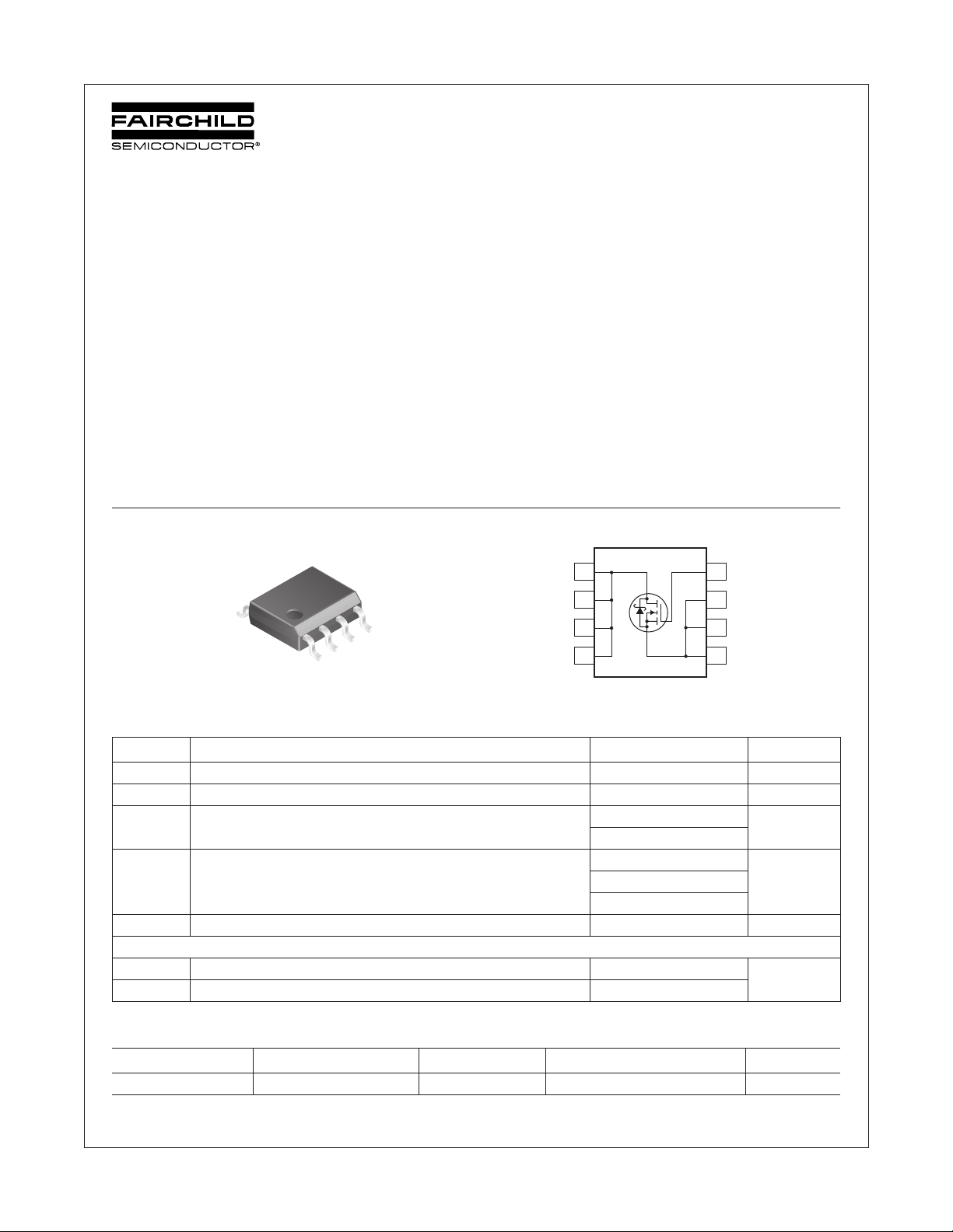
D
D
D
D
G
S
SO-8
S
S
General Description
The FDS6699S is designed to replace a single SO-8 MOSFET
and Schottky diode in synchronous DC:DC power supplies.
This 30V MOSFET is designed to maximize power conversion
efficiency, providing a low R
FDS6699S includes an integrated Schottky diode using Fairchild’s monolithic SyncFET technology.
5
6
7
8
and low gate charge. The
DS(ON)
4
3
2
1
®
SyncFET™
Absolute Maximum Ratings
T
=25°C unless otherwise noted
A
Symbol Parameter Ratings Units
V
DSS
V
GSS
I
D
P
D
, T
T
J
STG
Thermal Characteristics
R
JA
R
JC
Drain-Source Voltage
Gate-Source Voltage
Drain Current – Continuous (Note 1a)
– Pulsed 105
Power Dissipation for Single Operation (Note 1a)
(Note 1b) 1.2
(Note 1c) 1
Operating and Storage Junction Temperature Range
Thermal Resistance, Junction-to-Ambient (Note 1a)
Thermal Resistance, Junction-to-Case (Note 1) 25
30 V
21 A
2.5 W
–55 to +150
50
20 V
Package Marking and Ordering Information
Device Marking Device Reel Size Tape width Quantity
FDS6699S FDS6699S 13’’ 12mm 2500 units
©2005 Fairchild Semiconductor Corporation
FDS6699S Rev. D1
1
C/W
www.fairchildsemi.com
θ
θ
θ
∆
µ
∆
Ω
T
Electrical Characteristics
= 25°C unless otherwise noted
A
Symbol Parameter Test Conditions Min Typ Max Units
Off Characteristics
BV
DSS
BV
DSS
∆ T
J
I
DSS
I
GSS
On Characteristics (Note 2)
V
GS(th)
V
GS(th)
∆ T
J
R
DS(on)
g
FS
Dynamic Characteristics
C
iss
C
oss
C
rss
R
G
Switching Characteristics (Note 2)
t
d(on)
t
r
t
d(off)
t
f
Q
g(TOT)
Q
g
Q
gs
Q
gd
Drain–Source Diode Characteristics and Maximum Ratings
V
SD
t
rr
I
RM
Q
rr
Notes:
1. R
JA
R
JC
Drain–Source Breakdown Voltage V
Breakdown Voltage Temperature
Coefficient
Zero Gate Voltage Drain Current V
Gate–Body Leakage V
Gate Threshold Voltage V
Gate Threshold Voltage Temperature
Coefficient
Static Drain–Source
On–Resistance
Forward Transconductance V
Input Capacitance V
Output Capacitance 1050 pF
= 0 V, I
GS
I
= 1 mA, Referenced to 25 ° C28mV/ ° C
D
= 24 V, V
DS
= ±20 V, V
GS
= V
DS
I
= 1 mA, Referenced to 25 ° C –3.2 mV/ ° C
D
V
= 10 V, I
GS
V
= 4.5 V, I
GS
V
=10 V, I
GS
= 10 V, I
DS
= 15 V, V
DS
f = 1.0 MHz
= 1 mA 30 V
D
= 0 V 500
GS
= 0 V ±100 nA
DS
, I
= 1 mA 1 1.4 3 V
GS
D
= 21 A
D
= 19 A
D
=21 A, T
D
= 21 A 100 S
D
GS
= 0 V,
=150 ° C
J
3.0
3.6
4.6
3610 pF
3.6
4.5
5.6
m Ω
Reverse Transfer Capacitance 340 pF
Gate Resistance V
Tu r n–On Delay Time V
Tu r n–On Rise Time 12 22 ns
= 15 mV, f = 1.0 MHz 0.4 1.8 3.1
GS
DD
V
GS
= 15 V, I
= 10 V, R
= 1 A,
D
GEN
11 20 ns
= 6 Ω
Tu r n–Off Delay Time 73 117 ns
Tu r n–Off Fall Time 38 61 ns
Total Gate Charge at Vgs = 10V V
= 15 V, I
DD
= 21 A, 65 91 nC
D
Total Gate Charge at Vgs = 5V 35 49 nC
Gate–Source Charge 9nC
Gate–Drain Charge 11 nC
Drain–Source Diode Forward Voltage V
Diode Reverse Recovery Time I
Diode Reverse Recovery Current 2.2 A
GS
= 21 A,
F
d
/d
iF
= 0 V, I
= 3.5 A (Note 2) 0.36 0.7 V
S
= 300 A/µs (Note 3)
t
32 ns
Diode Reverse Recovery Charge 35 nC
is the sum of the junction-to-case and case-to-ambient thermal resistance where the case thermal reference is defined as the solder mounting surface of the drain pins.
is guaranteed by design while R
a) 50°/W when mounted
is determined by the user's board design.
CA
2
pad of 2 oz
on a 1 in
copper
b) 105°/W when mounted
on a .04 in
copper
2
pad of 2 oz
c) 125°/W when mounted
on a minimum pad.
FDS6699S 30V N-Channel PowerTrench
A
®
SyncFET™
Scale 1 : 1 on letter size paper
2. Pulse Test: Pulse Width < 300 µ s, Duty Cycle < 2.0%
3. See “SyncFET Schottky body diode characteristics” below.
FDS6699S Rev. D1
2
www.fairchildsemi.com
 Loading...