

Fairchild FDS6676AS service manual
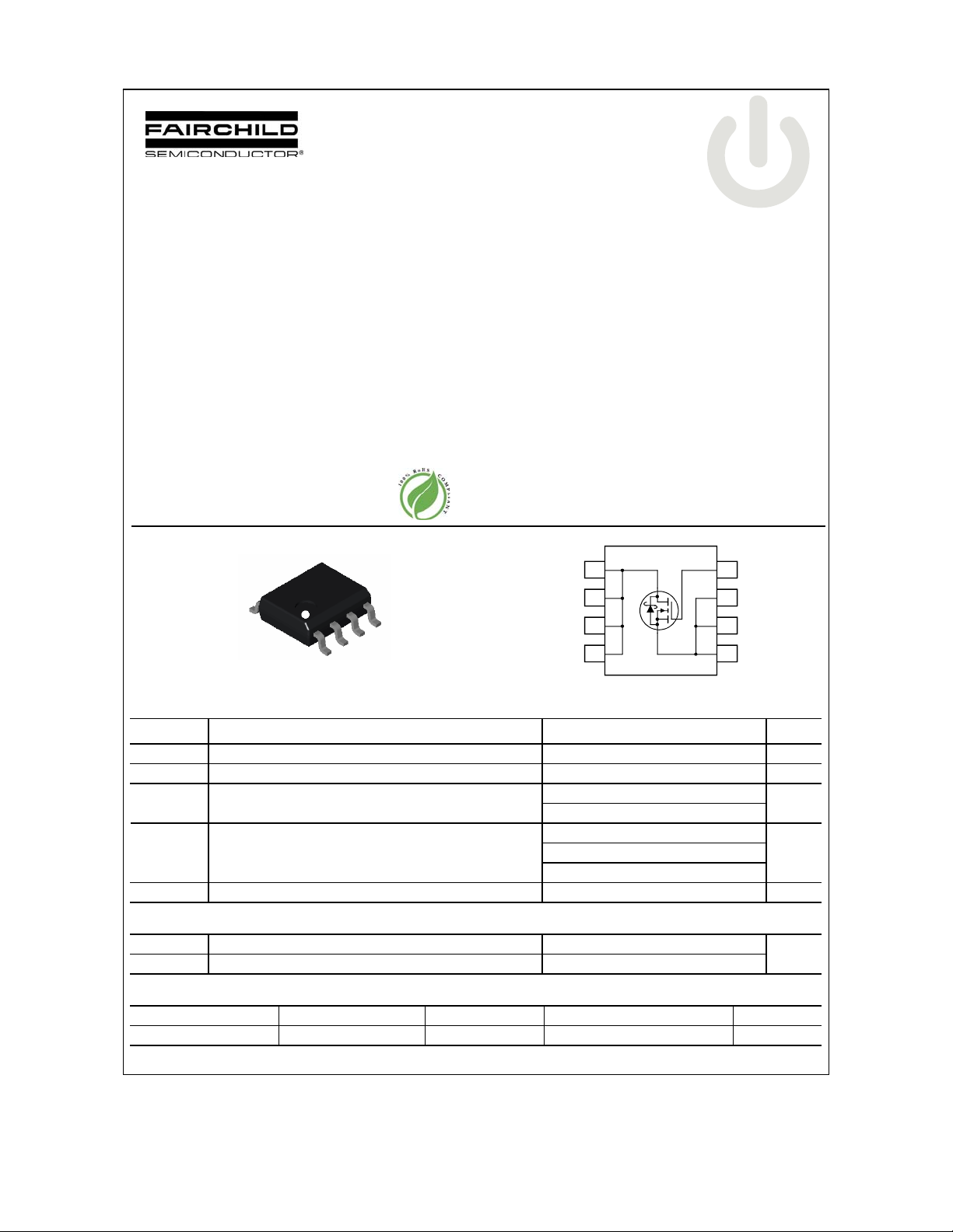
FDS6676AS
30V N-Channel PowerTrench® SyncFET™
May 2008
tm
FDS6676AS 30V N-Channel PowerTrench
General Description
The FDS6676AS is designed to replace a single SO-8
MOSFET and Schottky diode in synchronous DC:DC
power supplies. This 30V MOSFET is designed to
maximize power conversion efficiency, providing a low
R
and low gate charge. The FDS6676AS
DS(ON)
includes an integrated Schottky diode using Fairchild’s
monolithic SyncFET technology.
Applications
• DC/DC converter
• Low side notebook
D
D
D
D
G
S
SO-8
Absolute Maximum Ratings T
S
S
o
=25
C unless otherwise noted
A
Features
• 14.5 A, 30 V. R
R
• Includes SyncFET Schottky body diode
• Low gate charge (45nC typical)
• High performance trench technology for extremely low
and fast switching
R
DS(ON)
• High power and current handling capability
• RoHS Compliant
5
6
7
8
max= 6.0 mΩ @ V
DS(ON)
max= 7.25 mΩ @ V
DS(ON)
= 10 V
GS
= 4.5 V
GS
4
3
2
1
®
SyncFET™
Symbol Parameter Ratings Units
V
Drain-Source Voltage 30 V
DSS
V
Gate-Source Voltage
GSS
ID Drain Current – Continuous (Note 1a) 14.5 A
– Pulsed 50
PD
TJ, T
STG
Power Dissipation for Single Operation (Note 1a) 2.5
(Note 1b)
Operating and Storage Junction Temperature Range –55 to +150
(Note 1c)
±20
1.2
1
V
W
°C
Thermal Characteristics
R
θJA
R
θJC
Thermal Resistance, Junction-to-Ambient
Thermal Resistance, Junction-to-Case
(Note 1a) 50
(Note 1) 25
Package Marking and Ordering Information
Device Marking Device Reel Size Tape width Quantity
FDS6676AS FDS6676AS 13’’ 12mm 2500 units
F
©2008 Fairchild Semiconductor Corporation
DS6676AS Rev B
°C/W
2
FDS6676AS 30V N-Channel PowerTrench
Electrical Characteristics T
= 25°C unless otherwise noted
A
Symbol Parameter Test Conditions Min Typ Max Units
Off Characteristics
BV
Drain–Source Breakdown Voltage VGS = 0 V, ID = 1 mA 30 V
DSS
∆BVDSS
∆T
J
I
Zero Gate Voltage Drain Current VDS = 24 V, VGS = 0 V 500
DSS
I
Gate–Body Leakage
GSS
Breakdown Voltage Temperature
Coefficient
I
= 10 mA, Referenced to 25°C
D
= ±20 V, VDS = 0 V
V
GS
20
±100
mV/°C
µA
nA
On Characteristics (Note 2)
V
Gate Threshold Voltage VDS = VGS, ID = 1 mA 1 1.5 3 V
GS(th)
∆VGS(th)
∆TJ
R
DS(on)
I
On–State Drain Current VGS = 10 V, VDS = 5 V 50 A
D(on)
Gate Threshold Voltage
Temperature Coefficient
Static Drain–Source
On–Resistance
I
= 10 mA, Referenced to 25°C
D
VGS = 10 V, ID = 14.5 A
V
= 4.5 V, ID = 13.2 A
GS
=10 V, ID =14.5A, TJ=125°C
V
GS
–4
4.5
5.9
6.7
mV/°C
6.0
7.25
mΩ
8.5
gFS Forward Transconductance VDS = 10 V, ID = 14.5 A 66 S
Dynamic Characteristics
C
Input Capacitance 2510 pF
iss
C
Output Capacitance 710 pF
oss
C
Reverse Transfer Capacitance
rss
RG Gate Resistance VGS = 15 mV, f = 1.0 MHz 1.6 2.8
V
= 15 V, V
DS
f = 1.0 MHz
= 0 V,
GS
270 pF
Ω
Switching Characteristics (Note 2)
t
Turn–On Delay Time 10 20 ns
d(on)
tr Turn–On Rise Time 12 22 ns
t
Turn–Off Delay Time 43 69 ns
d(off)
tf Turn–Off Fall Time
t
Turn–On Delay Time 17 31 ns
d(on)
tr Turn–On Rise Time 22 35 ns
t
Turn–Off Delay Time 34 54 ns
d(off)
tf Turn–Off Fall Time
Q
g
(TOT)
Total Gate Charge at Vgs=10V 45 63 nC
Qg Total Gate Charge at Vgs=5V 25 35 nC
Qgs Gate–Source Charge 7 nC
Qgd Gate–Drain Charge
V
= 15 V, ID = 1 A,
DD
V
= 10 V, R
GS
V
= 15 V, ID = 1 A,
DD
V
= 4.5 V, R
GS
V
= 15 V, ID = 14.5 A,
DD
GEN
GEN
= 6 Ω
29 46 ns
= 6 Ω
29 46 ns
8 nC
®
SyncFET™
FDS6676AS Rev B2
FDS6676AS 30V N-Channel PowerTrench
Electrical Characteristics T
= 25°C unless otherwise noted
A
Symbol Parameter Test Conditions Min Typ Max Units
Drain–Source Diode Characteristics and Maximum Ratings
VSD Drain–Source Diode Forward
Voltage
trr Diode Reverse Recovery Time 27 nS
IRM Diode Reverse Recovery Current 1.9 A
Qrr Diode Reverse Recovery Charge
Notes:
1. R
is the sum of the junction-to-case and case-to-ambient thermal resistance where the case thermal reference is defined as the solder mounting surface of
θJA
the drain pins. R
is guaranteed by design while R
θJC
a) 50°/W when
mounted on a 1 in2
pad of 2 oz copper
θCA
VGS = 0 V, IS = 3.5 A (Note 2)
VGS = 0 V, IS = 7 A (Note 2)
I
= 14.5A,
F
d
= 300 A/µs (Note 3)
iF/dt
is determined by the user's board design.
b) 105°/W when
mounted on a .04 in
pad of 2 oz copper
2
0.4
0.7 V
0.5
26 nC
®
SyncFET™
FDS6676AS Rev B2
 Loading...