

FDS4672A
February 2007
FDS4672A
40V N-Channel PowerTrench® MOSFET
General Description
This N-Channel MOSFET has been designed
specifically to improve the overall efficiency of DC/DC
converters using either synchronous or conventional
switching PWM controllers. It has been optimized for
low gate charge, low R
Applications
• DC/DC converter
D
D
and fast switching speed.
DS(ON)
D
D
S
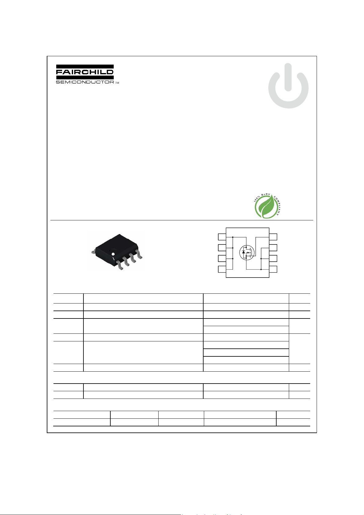
SO-8
S
S
G
Features
• 11 A, 40 V. R
• High performance trench technology for extremely
DS(ON)
5
6
7
8
low R
• Low gate charge (35 nC typical)
• High power and current handling capability
• RoHS Compliant
= 13 mΩ @ VGS = 4.5 V
DS(ON)
4
3
2
1
tm
Absolute Maximum Ratings T
o
=25
C unless otherwise noted
A
Symbol Parameter Ratings Units
V
Drain-Source Voltage 40 V
DSS
V
Gate-Source Voltage
GSS
ID Drain Current – Continuous (Note 1a) 11 A
– Pulsed 50
E
AS
PD
TJ, T
STG
Single Pulse Avalanche Energy (Note
Power Dissipation for Single Operation (Note 1a) 2.5
(Note 1b)
Operating and Storage Junction Temperature Range -55 to +175
3) 181
(Note 1c)
±12
mJ
1.4
1.2
V
W
°C
Thermal Characteristics
R
θJA
R
θJC
Thermal Resistance, Junction-to-Ambient
Thermal Resistance, Junction-to-Case
(Note 1a) 50
(Note 1) 25
°C/W
°C/W
Package Marking and Ordering Information
Device Marking Device Reel Size Tape width Quantity
FDS4672A FDS4672A 13’’ 12mm 2500 units
FDS4672A
©2007 Fairchild Semiconductor Corporation
Rev C1 (W)
FDS4672A
Electrical Characteristics T
= 25°C unless otherwise noted
A
Symbol Parameter Test Conditions Min Typ Max Units
Off Characteristics
BV
Drain–Source Breakdown Voltage
DSS
ΔBVDSS
ΔT
I
Zero Gate Voltage Drain Current VDS = 32 V, VGS = 0 V 1
DSS
I
GSSF
I
GSSR
Breakdown Voltage Temperature
Coefficient
J
Gate–Body Leakage, Forward VGS = 12 V, VDS = 0 V 100 nA
Gate–Body Leakage, Reverse VGS = –12 V VDS = 0 V –100 nA
= 0 V, ID = 250 μA
V
GS
= 250 μA, Referenced to 25°C
I
D
40 V
37
mV/°C
μA
On Characteristics (Note 2)
V
Gate Threshold Voltage
GS(th)
ΔVGS(th)
ΔTJ
R
DS(on)
I
D(on)
Gate Threshold Voltage
Temperature Coefficient
Static Drain–Source
On–Resistance
On–State Drain Current VGS = 4.5 V, VDS = 5 V 50 A
= VGS, ID = 250 μA
V
DS
= 250 μA, Referenced to 25°C
I
D
= 4.5 V, ID = 11 A
V
GS
=4.5 V, ID =11A, TJ=125°C
V
GS
gFS Forward Transconductance VDS = 5 V, ID = 11 A 65 S
0.8 1.2 2.0 V
–4
10
15
21
13
mV/°C
mΩ
Dynamic Characteristics
C
Input Capacitance 4766 pF
iss
C
Output Capacitance 346 pF
oss
C
Reverse Transfer Capacitance
rss
= 20 V, V
V
DS
f = 1.0 MHz
= 0 V,
GS
155 pF
Switching Characteristics (Note 2)
V
= 20 V, ID = 1 A,
t
Turn–On Delay Time 17 31 ns
d(on)
tr Turn–On Rise Time 9 18 ns
t
Turn–Off Delay Time 43 68 ns
d(off)
tf Turn–Off Fall Time
Qg Total Gate Charge 35 49 nC
Qgs Gate–Source Charge 7.8 nC
Qgd Gate–Drain Charge
DD
V
= 4.5 V, R
GS
= 20 V, ID = 11 A,
V
DS
V
= 4.5 V
GS
GEN
= 6 Ω
14 25 ns
8.8 nC
Drain–Source Diode Characteristics and Maximum Ratings
IS Maximum Continuous Drain–Source Diode Forward Current 2.1 A
VSD
Notes:
1. R
θJA
the drain pins. R
Drain–Source Diode Forward
Voltage
is the sum of the junction-to-case and case-to-ambient thermal resistance where the case thermal reference is defined as the solder mounting surface of
is guaranteed by design while R
θJC
θCA
VGS = 0 V, IS = 2.1 A (Note 2) 0.7 1.2 V
is determined by the user's board design.
a) 50°C/W when
mounted on a 1in
pad of 2 oz copper
Scale 1 : 1 on letter size paper
2. Pulse Test: Pulse Width < 300μs, Duty Cycle < 2.0%
3.Starting T
= 25oC, L = 3mH,ID = 11A, VDD = 40V, VGS = 10V
J
2
b) 105°C/W when
mounted on a .04 in
pad of 2 oz copper
2
c) 125°C/W when mounted on a
minimum pad.
FDS4672A Rev C1 (W)
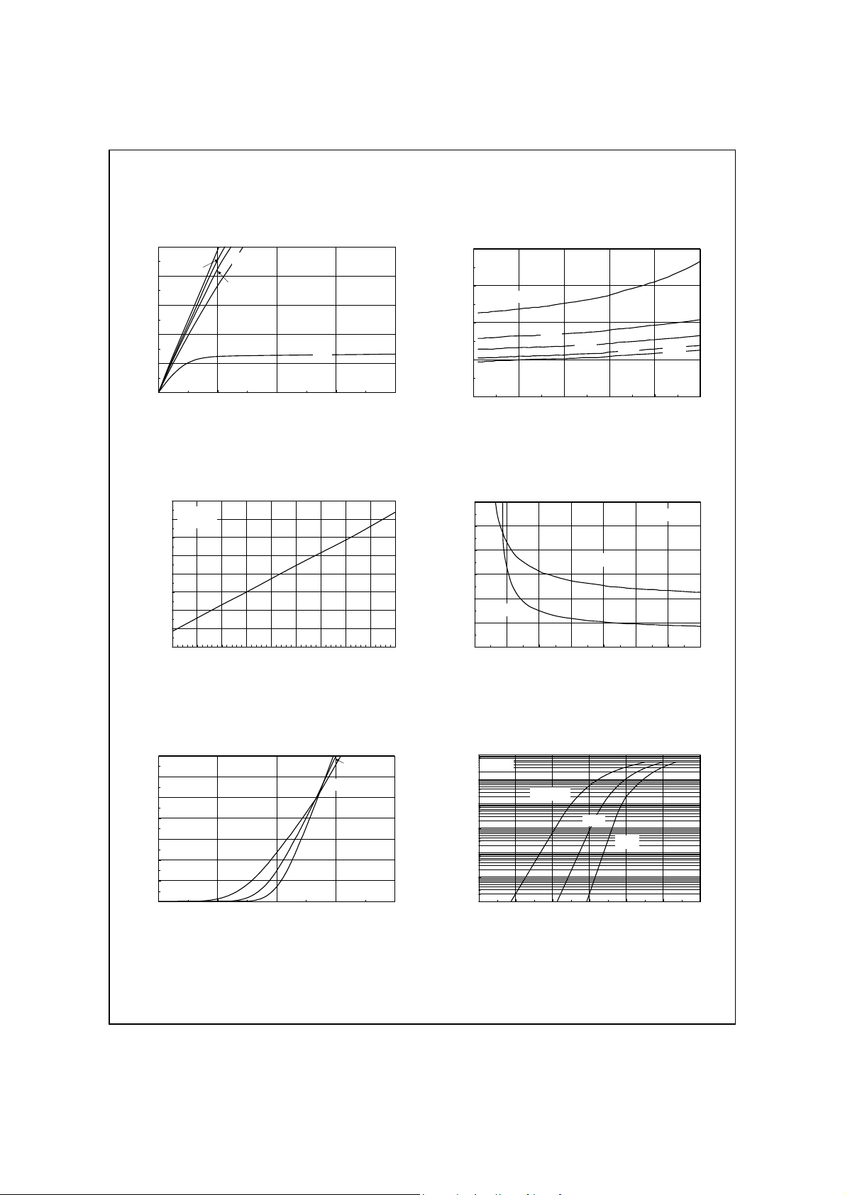
Typical Characteristics
FDS4672A
50
VGS = 4.5V
3.5V
40
30
20
, DRAIN CURRENT (A)
D
I
10
0
00.511.52
2.5V
3.0V
, DRAIN TO SOURCE VOLTAGE (V)
V
DS
2.0V
1.6
1.4
VGS = 2.5V
1.2
, NORMALIZED
DS(ON)
R
1
DRAIN-SOURCE ON-RESISTANCE
0.8
0 1020304050
3.0V
3.5V
I
, DRAIN CURRENT (A)
D
4.0V
Figure 1. On-Region Characteristics. Figure 2. On-Resistance Variation with
Drain Current and Gate Voltage.
2
ID = 11A
1.8
V
= 4.5V
GS
1.6
1.4
1.2
, NORMALIZED
1
DS(ON)
R
0.8
0.6
DRAIN-SOURCE ON-RESISTANCE
0.4
-50 -25 0 25 50 75 100 125 150 175
, JUNCTION TEMPERATURE (oC)
T
J
0.03
0.026
0.022
0.018
0.014
, ON-RESISTANCE (OHM)
R
TA = 25oC
DS(ON)
0.01
0.006
1.5 2 2.5 3 3.5 4 4.5 5
, GATE TO SOURCE VOLTAGE (V)
V
GS
TA = 125oC
4.5V
ID = 5.5A
Figure 3. On-Resistance Variation with
Temperature.
70
VDS = 5V
60
50
40
30
20
, DRAIN CURRENT (A)
D
I
10
0
11.522.53
, GATE TO SOURCE VOLTAGE (V)
V
GS
TA = -55oC 25oC
125oC
Figure 5. Transfer Characteristics. Figure 6. Body Diode Forward Voltage Variation
Figure 4. On-Resistance Variation with
Gate-to-Source Voltage.
100
VGS = 0V
10
1
0.1
0.01
0.001
, REVERSE DRAIN CURRENT (A)
S
I
0.0001
0 0.2 0.4 0.6 0.8 1 1.2
TA = 125oC
25oC
-55oC
BODY DIODE FORWARD VOLTAGE (V)
V
SD,
with Source Current and Temperature.
FDS4672A Rev C1 (W)

Typical Characteristics
FDS4672A
5
ID = 11A
4
3
2
1
, GATE-SOURCE VOLTAGE (V)
GS
V
0
0 10203040
Q
g
VDS = 10V
, GATE CHARGE (nC)
20V
30V
7000
5600
4200
2800
CAPACITANCE (pF)
1400
C
OSS
C
RSS
0
010203040
C
ISS
V
, DRAIN TO SOURCE VOLTAGE (V)
DS
Figure 7. Gate Charge Characteristics. Figure 8. Capacitance Characteristics.
100
100ms
1s
10ms
1ms
R
LIMIT
DS(ON)
10
1
VGS = 4.5V
SINGLE PULSE
, DRAIN CURRENT (A)
0.1
D
I
R
= 125oC/W
θJA
= 25oC
T
A
0.01
0.01 0.1 1 10 100
V
, DRAIN-SOURCE VOLTAGE (V)
DS
10s
DC
100μs
100
10
, AVALANCHE CURRENT (A)
AS
I
1
0.01 0.1 1 10 100 1000
125℃
t
, TIME IN AVALANCHE (mS)
AV
25℃
f = 1 MHz
V
= 0 V
GS
Figure 9. Maximum Safe Operating Area. Figure 10. Unclamped Inductive
Switching Capability.
50
40
30
20
SINGLE PULSE
R
125°C/W
=
θJA
25°C
T
=
A
10
P(pk),PEAK TRANSIENT POWER (W)
0
0.001 0.01 0.1 1 10 100
t
, TIME (sec)
1
Figure 11 Single Pulse Maximum Power Dissipation.
FDS4672A Rev C1 (W)
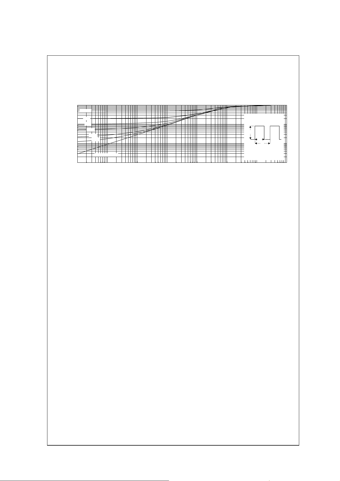
Typical Characteristics
1
D = 0.5
0.2
0.1
0.1
0.01
r(t), NORMALIZED EFFECTIVE
0.001
TRANSIENT THERMAL RESISTANCE
0.05
0.02
0.01
SINGLE PULSE
0.0001 0.001 0.01 0.1 1 10 100 1000
Figure 12. Transient Thermal Response Curve.
, TIME (sec)
t
1
Thermal characterization performed using the conditions described in Note 1c.
Transient thermal response will change depending on the circuit board design.
R
(t) = r(t) + R
JA
θ
R
= 125oC/W
JA
θ
P(pk)
t
1
t
2
T
- TA = P * R
J
Duty Cycle, D = t
FDS4672A
JA
θ
(t)
JA
θ
/ t
1
2
.
FDS4672A Rev C1 (W)
TRADEMARKS
The following are registered and unregistered trademarks Fairchild Semiconductor owns or is authorized to use and is not
intended to be an exhaustive list of all such trademarks.
ACEx™
ActiveArray™
Bottomless™
Build it Now™
CoolFET™
CROSSVOLT™
DOME™
EcoSPARK™
2
E
CMOS™
EnSigna™
®
FACT
®
FAST
FASTr™
FPS™
FRFET™
FACT Quiet Series™
GlobalOptoisolator™
GTO™
HiSeC™
2
I
C™
i-Lo™
ImpliedDisconnect™
IntelliMAX™
ISOPLANAR™
LittleFET™
MICROCOUPLER™
MicroFET™
MicroPak™
MICROWIRE™
MSX™
MSXPro™
Across the board. Around the world.™
The Power Franchise
®
OCX™
OCXPro™
OPTOLOGIC
®
OPTOPLANAR™
PACMAN™
POP™
Power247™
PowerEdge™
PowerSaver™
PowerTrench
QFET
®
®
QS™
QT Optoelectronics™
Quiet Series™
RapidConfigure™
RapidConnect™
µSerDes™
ScalarPump™
SILENT SWITCHER
SMART START™
SPM™
Stealth™
SuperFET™
SuperSOT™-3
SuperSOT™-6
SuperSOT™-8
SyncFET™
TCM™
TinyBoost™
TinyBuck™
TinyPWM™
TinyPower™
TinyLogic
®
TINYOPTO™
TruTranslation™
®
UHC
Programmable Active Droop™
DISCLAIMER
FAIRCHILD SEMICONDUCTOR RESERVES THE RIGHT TO MAKE CHANGES WITHOUT FURTHER NOTICE TO ANY PRODUCTS
HEREIN TO IMPROVE RELIABILITY, FUNCTION OR DESIGN. FAIRCHILD DOES NOT ASSUME ANY LIABILITY ARISING OUT OF THE
APPLICATION OR USE OF ANY PRODUCT OR CIRCUIT DESCRIBED HEREIN; NEITHER DOES IT CONVEY ANY LICENSE UNDER ITS
PATENT RIGHTS, NOR THE RIGHTS OF OTHERS. THESE SPECIFICATIONS DO NOT EXPAND THE TERMS OF FAIRCHILD’S
WORLDWIDE TERMS AND CONDITIONS, SPECIFICALLY THE WARRANTY THEREIN, WHICH COVERS THESE PRODUCTS.
®
UniFET™
VCX™
Wire™
LIFE SUPPORT POLICY
FAIRCHILD’S PRODUCTS ARE NOT AUTHORIZED FOR USE AS CRITICAL COMPONENTS IN LIFE SUPPORT DEVICES OR SYSTEMS
WITHOUT THE EXPRESS WRITTEN APPROVAL OF FAIRCHILD SEMICONDUCTOR CORPORATION.
As used herein:
1. Life support devices or systems are devices or systems
which, (a) are intended for surgical implant into the body, or
(b) support or sustain life, or (c) whose failure to perform
when properly used in accordance with instructions for use
provided in the labeling, can be reasonably expected to
result in significant injury to the user.
PRODUCT STATUS DEFINITIONS
Definition of Terms
2. A critical component is any component of a life support
device or system whose failure to perform can be
reasonably expected to cause the failure of the life support
device or system, or to affect its safety or effectiveness.
Datasheet Identification Product Status Definition
Advance Information Formative or In
Design
This datasheet contains the design specifications for
product development. Specifications may change in
any manner without notice.
Preliminary First Production This datasheet contains preliminary data, and
supplementary data will be published at a later date.
Fairchild Semiconductor reserves the right to make
changes at any time without notice in order to improve
design.
No Identification Needed Full Production This datasheet contains final specifications. Fairchild
Semiconductor reserves the right to make changes at
any time without notice in order to improve design.
Obsolete Not In Production This datasheet contains specifications on a product
that has been discontinued by Fairchild semiconductor.
The datasheet is printed for reference information only.
Rev. I22
 Loading...