

tm
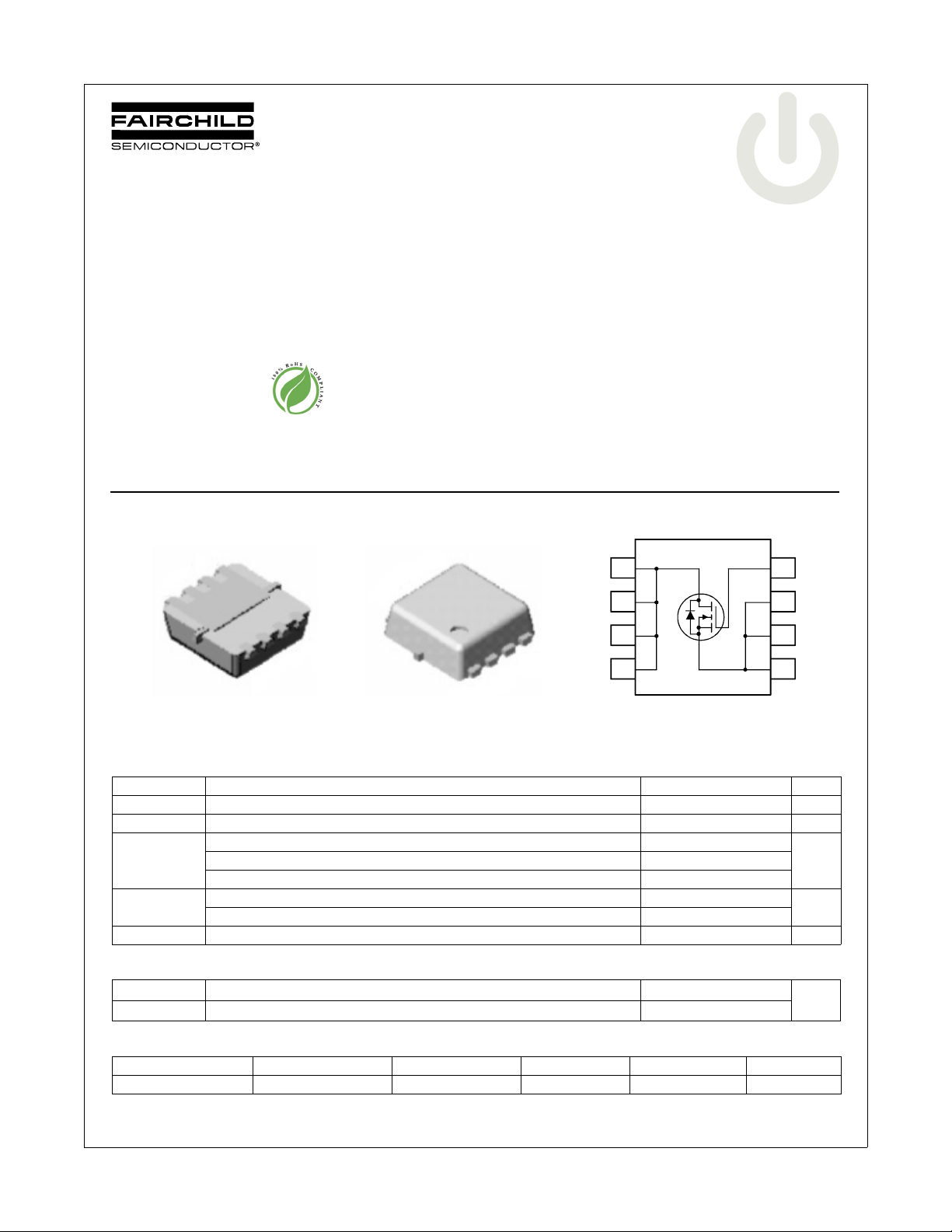
FDMC2610
N-Channel UltraFET Trench® MOSFET
200V, 9.5A, 200mΩ
Features
Max r
Max r
Low Profile - 1mm max in a Power 33
RoHS Compliant
= 200mΩ at VGS = 10V, ID = 2.2A
DS(on)
= 215mΩ at VGS = 6V, ID = 1.5A
DS(on)
General Description
This N-Channel MOSFET is a rugged gate version of
Fairchild Semiconductor‘s advanced Power Trench
process. It has been optimized for power management
applications.
Application
FDMC2610 N-Channel UltraFET Trench
January 2007
DC - DC Conversion
5
Bottom
7
6
8
D
1
2
3
4
Top
D
D
D
D
5
D
6
D
7
G
S
S
S
D
8
Power 33
MOSFET Maximum Ratings T
Symbol Parameter Ratings Units
V
DS
V
GS
I
D
P
D
, T
T
J
STG
Drain to Source Voltage 200 V
Gate to Source Voltage ±20 V
Drain Current -Continuous (Silicon limited) TC = 25°C 9.5
-Pulsed 15
Power Dissipation TC = 25°C 42
Power Dissipation T
Operating and Storage Junction Temperature Range -55 to +150 °C
= 25°C unless otherwise noted
A
= 25°C (Note 1a) 2.2
A
= 25°C (Note 1a) 2.1
A
Thermal Characteristics
®
MOSFET
G
4
S
3
2
S
S
1
A -Continuous T
W
R
θJC
R
θJA
Thermal Resistance, Junction to Case 3
Thermal Resistance, Junction to Ambient (Note 1a) 60
Package Marking and Ordering Information
Device Marking Device Package Reel Size Tape Width Quantity
FDMC2610 FDMC2610 Power 33 7’’ 8mm 3000 units
©2006 Fairchild Semiconductor Corporation
FDMC2610 Rev.C
°C/W
1
www.fairchildsemi.com
FDMC2610 N-Channel UltraFET Trench
Electrical Characteristics T
= 25°C unless otherwise noted
J
Symbol Parameter Test Conditions Min Typ Max Units
Off Characteristics
BV
DSS
ΔBV
DSS
ΔT
J
I
DSS
I
GSS
On Characteristics
V
GS(th)
ΔV
GS(th)
ΔT
J
r
DS(on)
g
FS
Drain to Source Breakdown Voltage ID = 250μA, VGS = 0V 200 V
Breakdown Voltage Temperature
Coefficient
Zero Gate Voltage Drain Current
Gate to Source Leakage Current VGS = ±20V, V
ID = 250μA, referenced to 25°C 199 mV/°C
VDS = 160V, 1
V
= 0V TJ = 125°C 100
GS
= 0V ±100 nA
DS
Gate to Source Threshold Voltage VGS = VDS, ID = 250μA 2 3.2 4 V
Gate to Source Threshold Voltage
Temperature Coefficient
Drain to Source On Resistance
Forward Transconductance VDS = 5V, ID = 2.2A 7 S
ID = 250μA, referenced to 25°C -9.9 mV/°C
VGS = 10V, ID = 2.2A 175 200
VGS = 10V, ID = 2.2A , TJ = 125°C 347 397
Dynamic Characteristics
C
iss
C
oss
C
rss
R
g
Input Capacitance
Output Capacitance 41 55 pF
Reverse Transfer Capacitance 12 20 pF
VDS = 100V, VGS = 0V,
f = 1MHz
720 960 pF
Gate Resistance f = 1MHz 0.7 Ω
μA
mΩVGS = 6V, ID = 1.5A 188 215
®
MOSFET
Switching Characteristics
t
d(on)
t
r
t
d(off)
t
f
Q
g(TOT)
Q
gs
Q
gd
Turn-On Delay Time
Rise Time 13 24 ns
Turn-Off Delay Time 29 47 ns
VDD = 100V, ID = 2.2A
VGS = 10V, R
GEN
Fall Time 16 29 ns
Total Gate Charge at 10V V
= 0V to 10V
GS
Gate to Source Gate Charge 3 nC
Gate to Drain “Miller” Charge 3.6 nC
Drain-Source Diode Characteristics
V
SD
t
rr
Q
rr
Notes:
1: R
is determined with the device mounted on a 1in2 pad 2 oz copper pad on a 1.5 x 1.5 in. board of FR-4 material. R
θJA
the user's board design.
2: Pulse Test: Pulse Width < 300μs, Duty cycle < 2.0%.
Source to Drain Diode Forward Voltage V
Reverse Recovery Time
Reverse Recovery Charge 11 4 171 nC
a. 60°C/W when mounted on
a 1 in2 pad of 2 oz copper
= 0V, IS = 2.2A (Note 2) 0.8 1.2 V
GS
IF = 2.2A, di/dt = 100A/μs
= 24Ω
VDD = 100V
ID = 2.2A
17 31 ns
12.3 18 nC
69 104 ns
is guaranteed by design while R
θJC
b. 135°C/W when mounted on a
minimum pad of 2 oz copper
is determined by
θCA
FDMC2610 Rev.C
2
www.fairchildsemi.com
FDMC2610 N-Channel UltraFET Trench
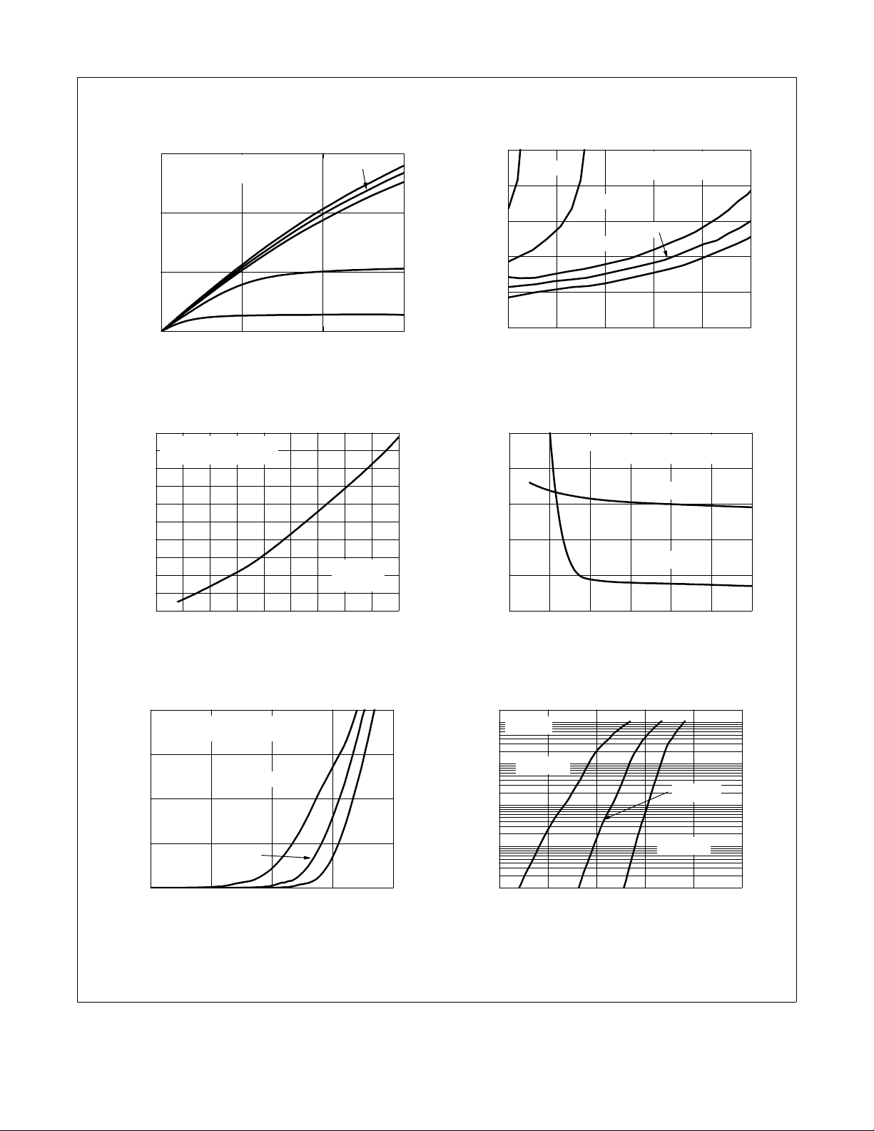
Typical Characteristics T
15
PULSE DURATION = 80μs
DUTY CYCLE = 0.5%MAX
VGS = 10V
10
5
, DRAIN CURRENT (A)
D
I
0
0123
VDS, DRAIN TO SOURCE VOLTAGE (V)
Figure 1.
On-Region Characteristics Figure 2.
2.4
PULSE DURATI ON = 80μs
2.2
DUTY CYCLE = 0.5%MAX
2.0
1.8
1.6
1.4
1.2
1.0
NORMALIZED
0.8
0.6
0.4
DRAIN TO SOURCE ON-RESISTANCE
-75 -50 -25 0 25 50 75 100 125 150
TJ, JUNCTION TEMPERATURE (oC)
F i g u r e 3 . N o r m a l i z e d O n - R e s i s t a n c e
vs Junction Temperature
VGS = 4.5V
= 25°C unless otherwise noted
J
V
= 7V
GS
VGS = 6V
V
= 5V
GS
ID =2.2A
V
= 10V
GS
1.8
V
= 4.5V
GS
1.6
1.4
1.2
NORMALIZED
1.0
0.8
DRAIN TO SOURCE ON-RESISTANCE
03691215
V
VGS = 10V
ID, DRAIN CURRENT(A)
PULSE DURATION = 80μs
DUTY CYCLE = 0.5%MAX
V
= 5V
GS
V
GS
= 6V
GS
= 7V
N o r m a l i z e d O n - R e s i s t a n c e
vs Drain Current and Gate Voltage
600
(mΩ)
500
400
, DRAIN TO
300
DS(on)
r
200
SOURCE ON-RESISTANCE
100
45678910
Figure 4.
ID = 1.4A
VGS, GATE TO SOURCE VOLTAGE (V)
PULSE DURATION = 80μs
DUTY CYCLE = 0.5%MAX
TA = 150oC
TA = 25oC
O n - R es i s t a n c e vs G a t e t o
Source Voltage
®
MOSFET
12
9
6
, DRAIN CURRENT (A)
3
D
I
0
FDMC2610 Rev.C
PULSE DURATION = 80μs
DUTY CYCLE = 0.5%MAX
TJ = 150oC
TJ = 25oC
23456
VGS, GATE TO SOURCE VOLTAGE (V)
TJ = -55oC
Figure 5. Transfer Characteristics
3
20
10
V
= 0V
GS
1
TJ = 150oC
0.1
0.01
, REVERSE DRAIN CURRENT (A)
S
I
1E-3
0.2 0.4 0.6 0.8 1.0 1.2
VSD, BODY DIODE FORWARD VOLTAGE (V)
Figure 6.
S o u r ce t o D r a i n Di o d e
TJ = 25oC
TJ = -55oC
Forward Voltage vs Source Current
www.fairchildsemi.com

FDMC2610 N-Channel UltraFET Trench
Typical Characteristics T
10
V
=50V
8
6
4
2
, GATE TO SOURCE VOLTAGE(V)
0
GS
V
03691215
Figure 7.
Gate Charge Characteristics Figure 8.
4
3
2
TJ = 125oC
, AVALANCHE CURRENT(A)
AS
I
1
-3
10
tAV, TIME IN AVALANCHE(ms)
Figure 9.
Switching Capability
40
r
DS(on)
LIMITED
10
1
0.1
, DRAIN CURRENT (A)
0.01
D
I
0.001
SINGLE PULSE
= MAX RATED
T
J
R
=135OC
θJA
T
= 25OC
A
0.1 1 10 100
VDS, DRAIN to SOURCE VOLTAGE (V)
F ig u re 1 1. F or w ar d B ia s Sa f e
DD
Qg, GATE CHARGE(nC)
-2
10
U n c l a m p e d I n d u c t i v e
Operating Area
= 25°C unless otherwise noted
J
VDD = 100V
VDD = 150V
TJ = 25oC
-1
10
100us
1ms
10ms
100ms
1s
DC
700
0
10
1000
C
iss
100
C
oss
CAPACITANCE (pF)
f = 1MHz
= 0V
V
GS
10
0.1 1 10 100
VDS, DRAIN TO SOURCE VOLTAGE (V)
C
rss
C a p a c i t a n c e v s D r a i n
to Source Voltage
10
8
V
= 10V
GS
6
V
= 6V
GS
4
, DRAIN CURRENT (A)
D
I
2
R
= 3oC/W
θJC
0
25 50 75 100 125 150
TC, CASE TEMPERATURE (oC)
Figure 10.
M a x i m u m C o n t i n u o u s D r a i n
Current vs Case Temperature
500
VGS = 10V
100
10
SINGLE PULSE
), PEAK TRANSIENT POWER (W)
1
PK
0.5
P(
10-410-310-210-110010110210
O
R
=135
C
θJA
t, PULSE WIDTH (s)
Figure 12.
S i n g l e P u l s e M a x i m u m
TA = 25oC
FOR TEMPERATURES
o
I = I
25
C DERATE PEAK
150 TA–
------------------------
ABOVE 25
CURRENT AS FOLLOWS:
Power Dissipation
®
MOSFET
125
3
FDMC2610 Rev.C
4
www.fairchildsemi.com

FDMC2610 N-Channel UltraFET Trench
Typical Characteristics T
2
DUTY CYCLE-DESCENDI NG ORDER
1
D = 0.5
0.2
θJA
0.1
0.05
0.02
0.1
0.01
IMPEDANCE, Z
0.01
NORMALIZED THERMAL
0.003
SINGLE PULSE
-3
10
-2
10
= 25°C unless otherwise noted
J
NOTES:
DUTY FACTOR: D = t
PEAK TJ = PDM x Z
-1
10
0
10
1
10
t, RECTANGULAR PULSE DURATION(s)
Figure 13. Transient Thermal Response Curve
P
θJA
10
DM
t
1
t
2
1/t2
x R
+ T
θJA
A
2
3
10
®
MOSFET
FDMC2610 Rev.C
5
www.fairchildsemi.com

FDMC2610 N-Channel UltraFET Trench
®
MOSFET
FDMC2610 Rev.C
6
www.fairchildsemi.com

TRADEMARKS
The following are registered and unregistered trademarks Fairchild Semiconductor owns or is authorized to use and is not
intended to be an exhaustive list of all such trademarks.
ACEx™
ActiveArray™
Bottomless™
Build it Now™
CoolFET™
CROSSVOLT™
DOME™
EcoSPARK™
2
E
CMOS™
EnSigna™
®
FACT
®
FAST
FASTr™
FPS™
FRFET™
FACT Quiet Series™
GlobalOptoisolator™
GTO™
HiSeC™
2
I
C™
i-Lo™
ImpliedDisconnect™
IntelliMAX™
ISOPLANAR™
LittleFET™
MICROCOUPLER™
MicroFET™
MicroPak™
MICROWIRE™
MSX™
MSXPro™
Across the board. Around the world.™
The Power Franchise
®
OCX™
OCXPro™
OPTOLOGIC
®
OPTOPLANAR™
PACMAN™
POP™
Power247™
PowerEdge™
PowerSaver™
PowerTrench
QFET
®
®
QS™
QT Optoelectronics™
Quiet Series™
RapidConfigure™
RapidConnect™
µSerDes™
ScalarPump™
SILENT SWITCHER
SMART START™
SPM™
Stealth™
SuperFET™
SuperSOT™-3
SuperSOT™-6
SuperSOT™-8
SyncFET™
TCM™
TinyBoost™
TinyBuck™
TinyPWM™
TinyPower™
TinyLogic
®
TINYOPTO™
TruTranslation™
®
UHC
Programmable Active Droop™
DISCLAIMER
FAIRCHILD SEMICONDUCTOR RESERVES THE RIGHT TO MAKE CHANGES WITHOUT FURTHER NOTICE TO ANY PRODUCTS HEREIN TO
IMPROVE RELIABILITY, FUNCTION OR DESIGN. FAIRCHILD DOES NOT ASSUME ANY LIABILITY ARISING OUT OF THE APPLICATION OR USE
OF ANY PRODUCT OR CIRCUIT DESCRIBED HEREIN; NEITHER DOES IT CONVEY ANY LICENSE UNDER ITS PATENT RIGHTS, NOR THE
RIGHTS OF OTHERS. THESE SPECIFICATIONS DO NOT EXPAND THE TERMS OF FAIRCHILD’S WORLDWIDE TERMS AND CONDITIONS,
SPECIFICALLY THE WARRANTY THEREIN, WHICH COVERS THESE PRODUCTS.
®
UniFET™
VCX™
Wire™
FDMC2610 N-Channel UItraFET Trench
®
MOSFET
LIFE SUPPORT POLICY
FAIRCHILD’S PRODUCTS ARE NOT AUTHORIZED FOR USE AS CRITICAL COMPONENTS IN LIFE SUPPORT DEVICES OR SYSTEMS WITHOUT
THE EXPRESS WRITTEN APPROVAL OF FAIRCHILD SEMICONDUCTOR CORPORATION.
As used herein:
1. Life support devices or systems are devices or systems which,
(a) are intended for surgical implant into the body, or (b) support
or sustain life, or (c) whose failure to perform when properly used
in accordance with instructions for use provided in the labeling,
can be reasonably expected to result in significant injury to the
2. A critical component is any component of a life support device
or system whose failure to perform can be reasonably expected
to cause the failure of the life support device or system, or to
affect its safety or effectiveness.
user.
PRODUCT STATUS DEFINITIONS
Definition of Terms
Datasheet Identification Product Status Definition
Advance Information Formative or In
Design
This datasheet contains the design specifications for
product development. Specifications may change in
any manner without notice.
Preliminary First Production This datasheet contains preliminary data, and
supplementary data will be published at a later date.
Fairchild Semiconductor reserves the right to make
changes at any time without notice in order to improve
design.
No Identification Needed Full Production This datasheet contains final specifications. Fairchild
Semiconductor reserves the right to make changes at
any time without notice in order to improve design.
Obsolete Not In Production This datasheet contains specifications on a product
that has been discontinued by Fairchild semiconductor.
The datasheet is printed for reference information only.
FDMC2610 Rev. C
Rev. I22
7
www.fairchildsemi.com
 Loading...