www.fairchildsemi.com
AN-8023
Negative Voltage Management Using a
FAN8303 Buck Regulator
for linear regulators in PC monitor and TV applications. In
Abstract
FAN8303 is a 2A, 370kHz monolithic integrated buck
regulator with internal power MOSFETs. It is simple to use
and needs minimal external components. This application
note describes how to generate negative voltage using
FAN8303. It introduces application examples and discusses
optimized designs for a buck-boost circuit.
Introduction
Buck regulators are widely used for higher voltage to lower
voltage DC conversion. Likewise, FAN8303 was originally
designed for application needing regulated DC voltage, such
as set-top box microcontrollers and efficient pre-regulators
some cases, a non-synchronous buck regulator also can be
utilized for buck-boost circuit to generate negative voltage
with respect to ground. These applications include audio
amplifier, timing control circuit for LCD panel, and so on.
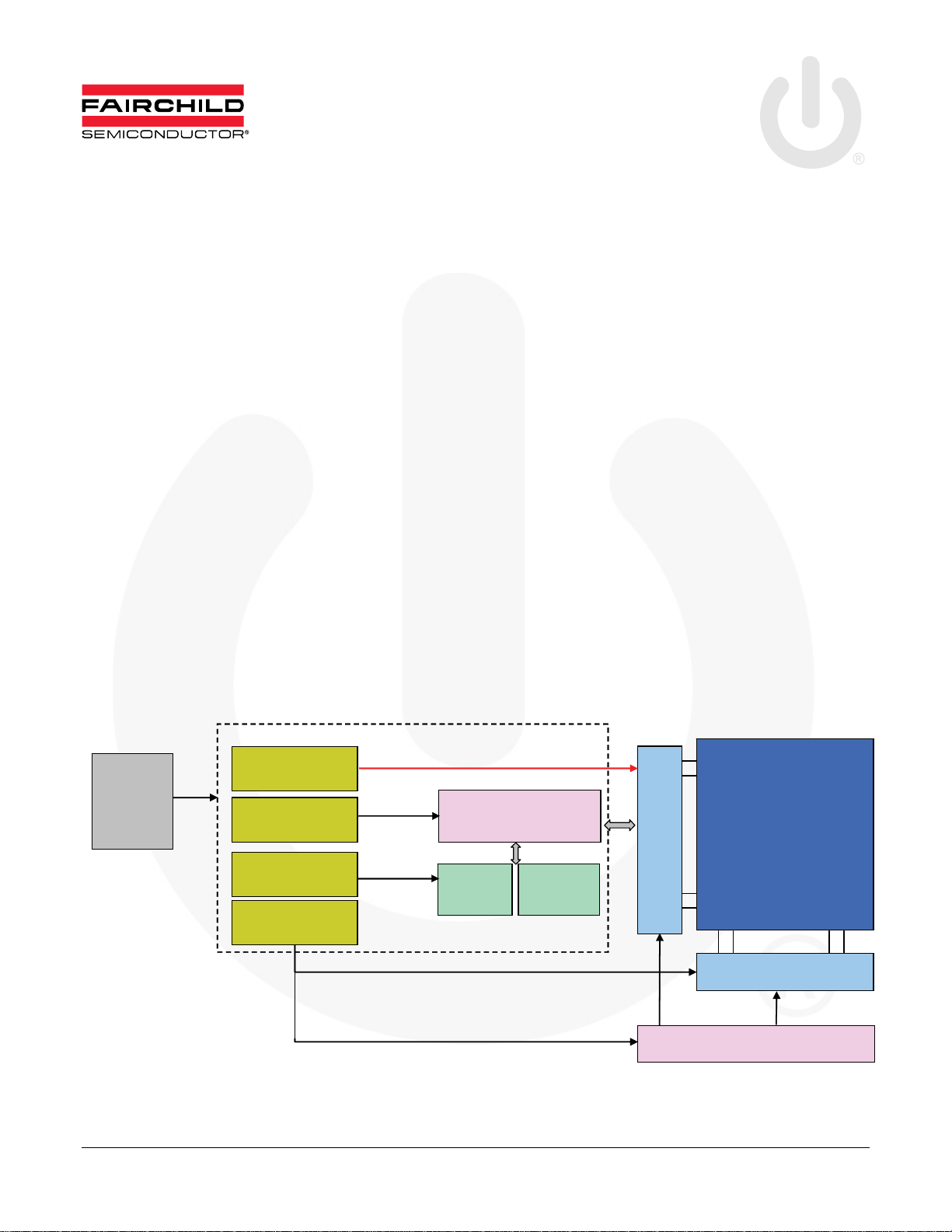
Figure 1 shows a practical application of an LCD panel; it
needs negative voltage for contrast control. In this block
diagram, a charge pump is usually adopted due to the simple
design and low cost. However, it has an amount of power
dissipation and poor output voltage regulation relative to
input voltage variation. FAN8303 with negative output
would be a solution to overcome these problems.
Charge pump
12V
AV Board
LDO
DC/DC (buck)
DC/DC (boost)
16V
© 2009 Fairchild Semiconductor Corporation www.fairchildsemi.com
Rev. 1.0.0 • 7/30/09
2.5V, 3.3V
2.5V
Figure 1. Example of Timing Control Block
-5V , 15V
DDR2
SoC
EEPROM
TFT LCD Panel
Row Drivers
Column Drivers
P-gamma IC

AN-8023 APPLICATION NOTE
V
V
T
D
I
Principle of Operation
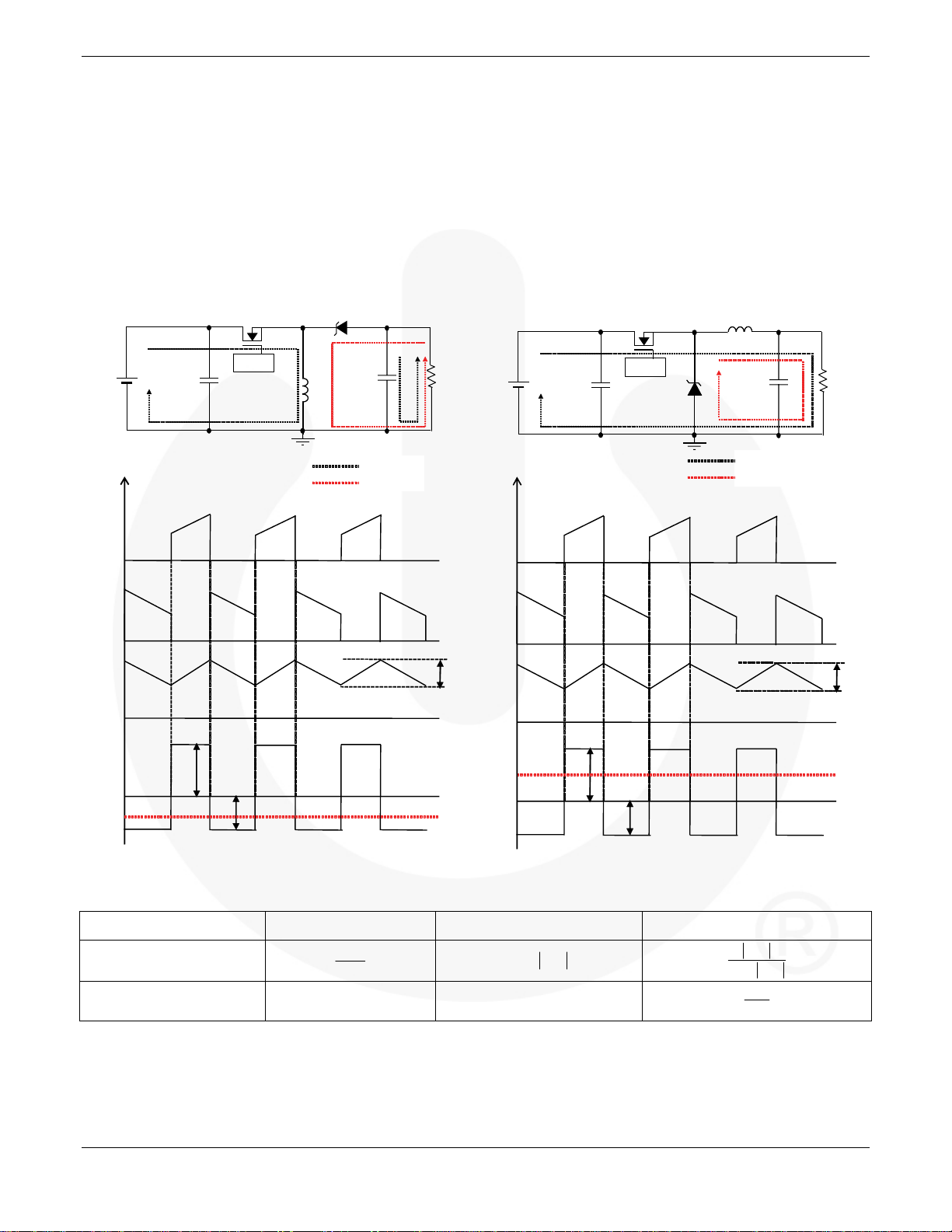
To understand buck-boost topology, buck topolgy is briefly
compared below. When the MOSFET switch (Q1 in Figure 3)
is turned on, the voltage across inductor (V
During Q1 off-time, V
the inductor current (I
ramps down with V
is equal to -V
L
) ramps up with (VIN-V
L
/L slope. Thus, the energy can be
OUT
) is V
L
IN -VOUT
in buck topology. So
OUT
)/L and
OUT
.
transferred to the load with positive output voltage.
Meanwhile, in buck-boost topology, the inductor and
freewheeling diode switch positions. When the MOSFET
Q1
PWM
IN
I
1Q
I
1D
C
IN
D1
C
L
OUT
OUT
Q1 ON
Q1 OFF
V
o
Load
t
switch Q1 (Figure 2) is turned on, V
is same as VIN, so I
L
ramps up with VIN/L. During the Q1 off-time, VL has reverse
polarity to maintain continuous inductor current with -V
Therefore, it can generate negative output voltage.
Buck-boost circuit with buck regulators require several
design considerations. Table 1 summarizes the design
parameter comparison between buck and buck-boost circuit.
L
Q1
PWM
IN
C
IN
OUT
C
D1
OUT
Q1 ON
Q1 OFF
I
1Q
I
1D
L
.
OUT
Vo
Load
t
I
L
I∆
L
V
L
V
IN
V−
OUT
V
OUT
Figure 2. Buck-Boost Topology Figure 3. Buck Topology
Table 1. Buck and Buck-Boost Design Parameters
Topology I
Buck-Boost
Buck
(Average) Maximum VSW Duty Cycles
L
I
OUT
1
−
OUT
First of all, inductor current is limited by (1–D); so attention
is needed to see that the maximum output current of buck
regulator is be always lower than the maximum current in
buck-boost circuit. Second, the switch node is a sum of input
voltage and output voltage in buck-boost. It also needs to be
I
L
V
L
VV−
IN OUT
V−
OUT
V
VV+
IN OUT
V
IN
limited to the maximum switch node voltage of buck
regulator. Since buck-boost is very noisy on input and
output compared to buck circuit, it requires good-quality
MLCC as input and output filters.
OUT
VV+
IN OUT
V
OUT
V
IN
I∆
L
V
OU
© 2009 Fairchild Semiconductor Corporation www.fairchildsemi.com
Rev. 1.0.0 • 7/30/09 2
 Loading...