November 2008
FAN8301
2A, 16V, Non-Synchronous, Step-Down, DC/DC Regulator
FAN8301 — 2A, 16V, Non-Synchronous, Step-Down, DC/DC Regulator
Features
2A Output Current
0.22Ω Internal Power MOSFET Switch
Wide 4.75V to 16V Operating Input Range
Output Adjustable from 0.6 to 14V
Stable with Low-ESR Output Ceramic Capacitors
Up to 90% Efficiency
Less than 20µA Shutdown Current
Fixed 370kHz Frequency
Thermal Shutdown with Hysteresis
Cycle-by-Cycle Over-Current Protection
Available in 8-Pin SOIC Package
Applications
Set-Top Boxes
DSL and Cable Modems
Distributed Power Systems
Consumer Appliances (DVD)
Auxiliary Supplies
Description
The FAN8301 is a monolithic, non-synchronous, stepdown (buck) regulator with internal power MOSFETs. It
achieves 2A continuous output current over a wide input
supply range with excellent load and line regulation.
Current-mode operation provides fast transient
response and eases loop stabilization. Fault condition
protection includes cycle-by-cycle current limiting and
thermal shutdown. The regulator draws less than 20µA
shutdown current. The FAN8301 requires a minimum
number of readily available standard external
components.
External compensation, enable, and programmable
soft-start features allow design optimization and
flexibility. Cycle-by-cycle current limit, frequency
foldback, and thermal shutdown provide protection
against shorted outputs.
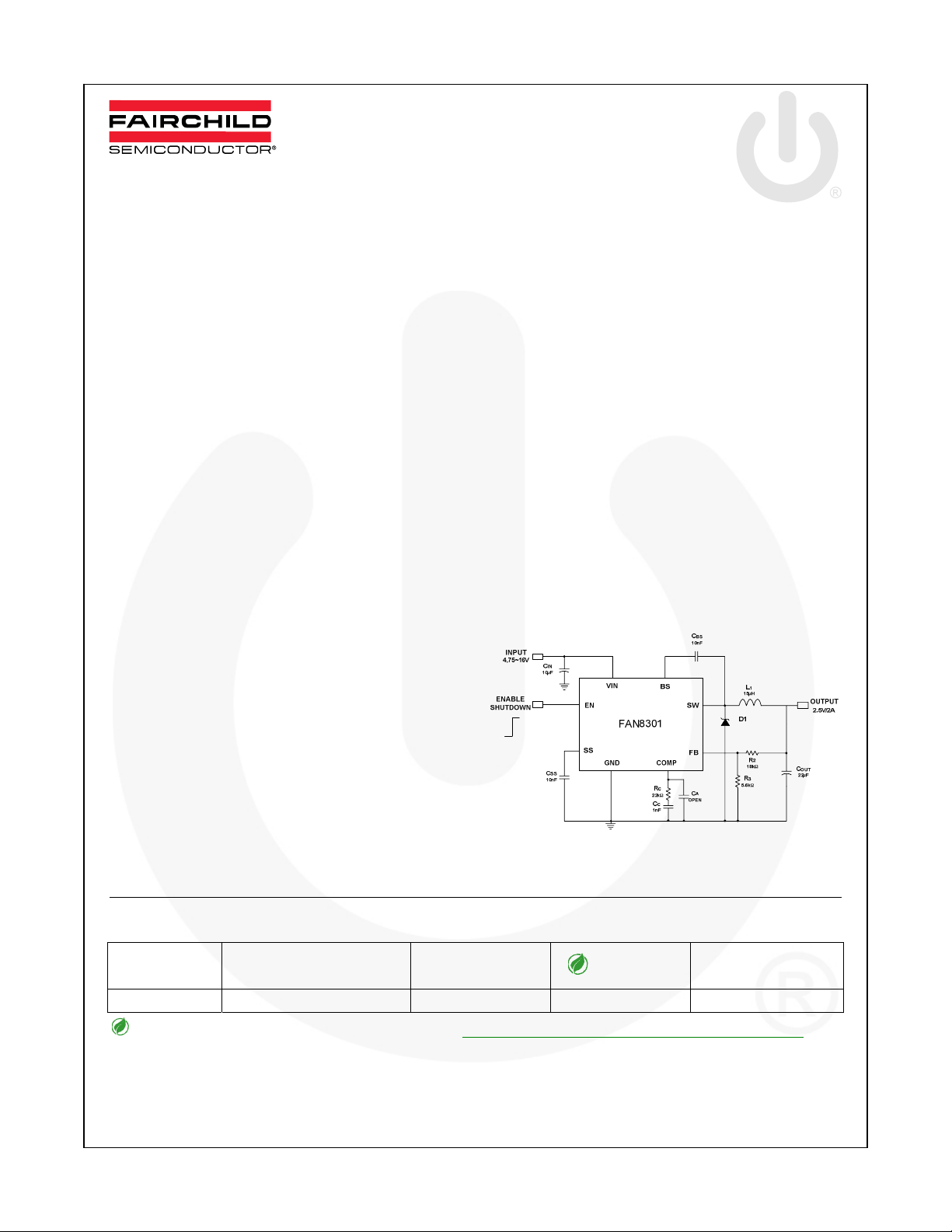
Figure 1. Typical Application
Ordering Information
Part Number
FAN8301MX -40°C to +85°C 8-SOIC RoHS Reel
For Fairchild’s definition of “green” Eco Status, please vis i t : http://www.fairchildsemi.com/company/green/rohs_green.html.
© 2008 Fairchild Semiconductor Corporation www.fairchildsemi.com
FAN8301 • Rev. 1.0.0
Operating
Temperature Range
Package
Eco Status
Packing Method

Internal Block Diagram
FAN8301 — 2A, 16V, Non-Synchronous, Step-Down, DC/DC Regulator
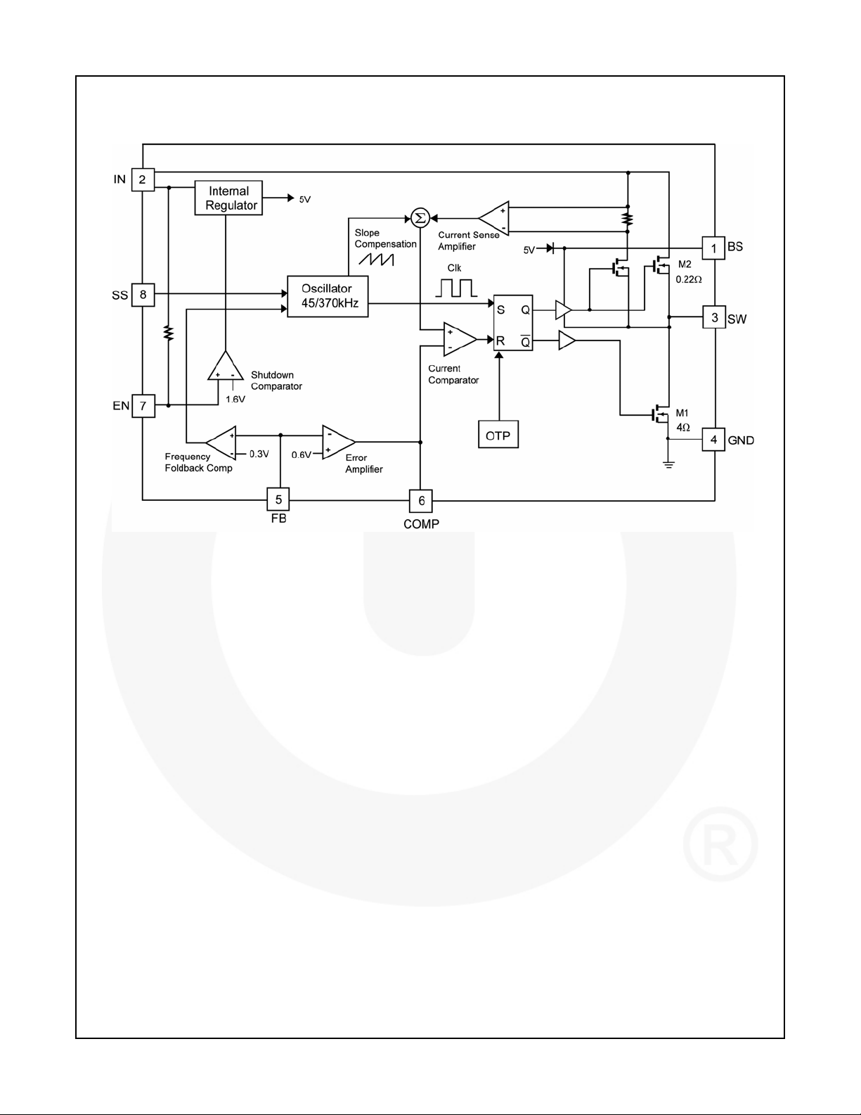
Figure 2. Functional Block Diagram
© 2008 Fairchild Semiconductor Corporation www.fairchildsemi.com
FAN8301 • Rev. 1.0.0 2

Pin Configuration
V
FAN8301 — 2A, 16V, Non-Synchronous, Step-Down, DC/DC Regulator
BS
IN
SW
GND
SS
EN
COMP
FB
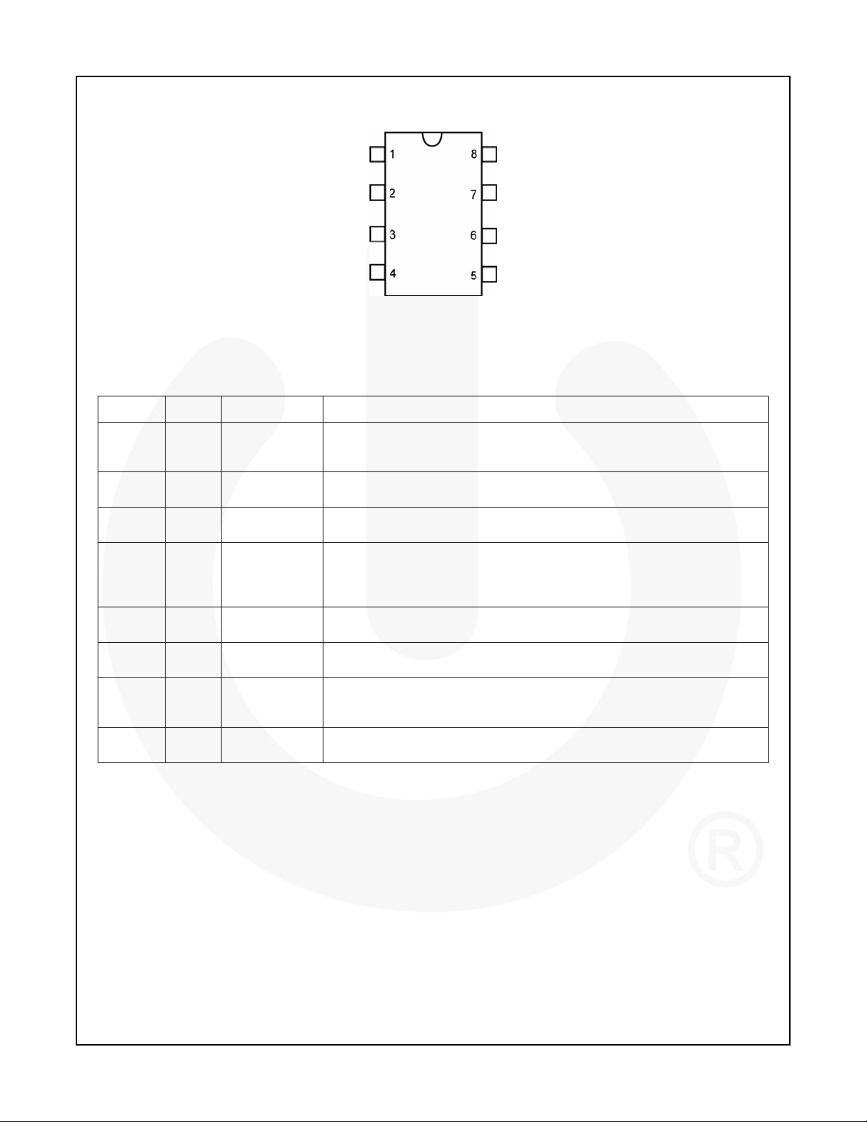
Figure 3. Pin Configuration (Top View)
Pin Definitions
Name Pin # Type Description
High-Side Drive BOOT Voltage. Connect through capacitor (C
BS 1 Bootstrap
VIN 2 Supply Voltage
SW 3 Switch
GND 4 Ground
FB 5 Feedback
COMP 6 Compensation
EN 7 Enable
SS 8 Soft-Start
IC includes an internal synchronous bootstrap diode to recharge the
capacitor on this pin to V
Power Input. This pin needs to be closely decoupled to GND pin with a 10µF
or greater ceramic capacitor.
Power Switching Output. SW is the switching node that supplies power to the
output.
The power return and signal ground for the IC. All internal control voltages
are referred to this pin. Tie this pin to the ground island/plane through the
lowest impedance connection. This pin is the ground reference for the
regulated output voltage.
Feedback Input. The center tap of the external feedback voltage resistive
divider across the output.
Compensation Node. Frequency compensation is accomplished at this node
by connecting a series R-C to ground.
Enable Input. EN is a digital input that turns the regulator on or off. Drive EN
HIGH to turn on the regulator, drive it LOW to turn it off. For automatic
startup, leave EN unconnected.
External Soft-Start. A capacitor connected between this pin and GND can be
used to set soft-start time.
when SW is LOW.
CC
) to SW. The
BS
© 2008 Fairchild Semiconductor Corporation www.fairchildsemi.com
FAN8301 • Rev. 1.0.0 3

FAN8301 — 2A, 16V, Non-Synchronous, Step-Down, DC/DC Regulator
Absolute Maximum Ratings
Stresses exceeding the absolute maximum ratings may damage the device. The device may not function or be
operable above the recommended operating conditions and stressing the parts to these levels is not recommended.
In addition, extended exposure to stresses above the recommended operating conditions may affect device
reliability. The absolute maximum ratings are stress ratings only. All voltage values, except differential voltages, are
given with respect to the network ground terminal. Stresses beyond those listed under Absolute Maximum Ratings
may cause permanent damage to the device
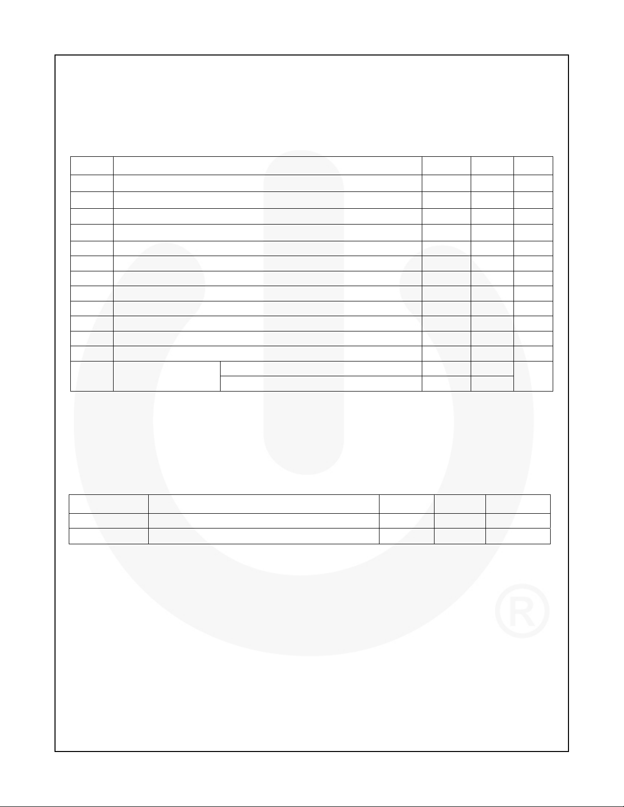
Symbol Parameter Min. Max. Unit
VIN Supply Voltage, VIN to GND 18 V
VSW Switch Voltage, SW to GND -0.3 VIN+0.3 V
VBS Boost Voltage VSW+6.0 V
VFB Feedback Voltage -0.3 6.0 V
VEN Enable Voltage -0.3 6.0 V
V
Compensation Voltage -0.3 6.0 V
COMP
VSS Soft-Start Voltage -0.3 6.0 V
JA Thermal Resistance, Junction-to-Air 105 °C/W
JC Thermal Resistance, Junction-to-Case 40 °C/W
TJ Operating Junction Temperature -40 +125 °C
TL Lead Temperature (Soldering, 5 Seconds) +260 °C
T
Storage Temperature Range -65 +150 °C
STG
ESD
Electrostatic Discharge
Protection Level
Human Body Model, JEDEC JESD22-A114 2.5
Charged Device Model, JEDEC JESD22-C101 2.5
kV
Recommended Operating Conditions
The Recommended Operating Conditions table defines the conditions for actual device operation. Recommended
operating conditions are specified to ensure optimal performance to the datasheet specifications. Fairchild does not
recommend exceeding them or designing to absolute maximum ratings.
Symbol Parameter Min Max. Unit
VIN Supply Voltage 4.75 16.00 V
TA Operating Ambient Temperature -40 +85
°C
© 2008 Fairchild Semiconductor Corporation www.fairchildsemi.com
FAN8301 • Rev. 1.0.0 4
 Loading...