Fairchild FAN7602C service manual

FAN7602C
Green Current Mode PWM Controller
FAN7602C — Green Current Mode PWM Controller
April 2009
Features
Green Current Mode PWM Controller
Random Frequency Fluctuation for Low EMI
Internal High-Voltage Startup Switch
Burst Mode Operation
Line Voltage Feedforward to Limit Maximum Power
Line Under-Voltage Protection
Latch Protection & Internal Soft-Start (10ms) Function
Overload Protection
Over-Voltage Protection
Over-Temperature Protection
Low Operation Current: 1mA Typical
8-Pin DIP/SOP
Applications
Adapter
LCD Monitor Power
Auxiliary Power Supply
Related Resources
AN-6014- Green Current Mode PWM Controller
(Except for frequency fluctuation part in AN-6014)
Description
The FAN7602C is a green current-mode PWM controller.
It is specially designed for off-line adapter applications;
DVDP, VCR, LCD monitor applications; and auxiliary
power supplies.
The internal high-voltage startup switch and the burst
mode operation reduce the power loss in standby mode.
As a result, the input power is lower than 1W when the
input line voltage is 265V
load condition, input power is under 0.15W.
The maximum power can be limited constantly,
regardless of the line voltage change, using the power
limit function.
The switching frequency is not fixed and it has random
frequency fluctuation.
The FAN7602C includes various protections for the
system reliability and the internal soft-start prevents the
output voltage over-shoot at startup.
and the load is 0.5W. At no-
AC
Ordering Information
Part Number
FAN7602CN 8-DIP Rail FAN7602C
FAN7602CM Rail FAN7602C
FAN7602CMX
For Fairchild’s definition of Eco Status, please visit: http://www.fairchildsemi.com/company/green/rohs_green.html.
© 2009 Fairchild Semiconductor Corporation www.fairchildsemi.com
FAN7602C • Rev. 1.0.0
Operating Junction
Temperature
-40°C to +150°C RoHS
Eco Status
Package
8-SOP
Packing
Method
Tape and Reel FAN7602C
Top Mark

Typical Application Diagram
FAN7602C — Green Current Mode PWM Controller
Internal Block Diagram
LUVP
1
2V/1.5V
LUVP
Latch
LUVP
Latch/
Plimit
CS/FB
GND
FAN7602C
V
NC
V
Out
STR
CC
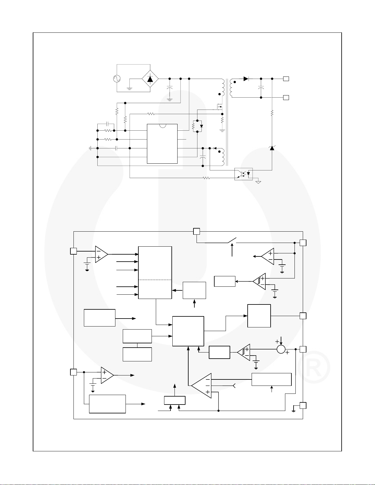
Figure 1. Typical Flyback Application
V
STR
8
OLP
TSD
OVP
Auto Restart
Protection
Latch
Protection
Reset
Circuit
SS End
5V Ref
OVP
UVLO
19V
12V/8V
6
V
CC
Vcc
Soft
Start
Driver
Circuit
Power Limit
Plimit
Offset
Plimit
Offset
5
3
4
OUT
CS/FB
GND
Latch/
Plimit
10ms
SS End
Soft Start
PWM
OSC
Block
Delay
Random
Circuit
0.95V/0.88V
2
Latch
PWM+
OLP
4V
Plimit
Offset
Generator
Plimit
Offset
OLP
Soft
Start
Figure 2. Functional Block Diagram
© 2009 Fairchild Semiconductor Corporation www.fairchildsemi.com
FAN7602C • Rev. 1.0.0 2

Pin Configuration
FAN7602C — Green Current Mode PWM Controller
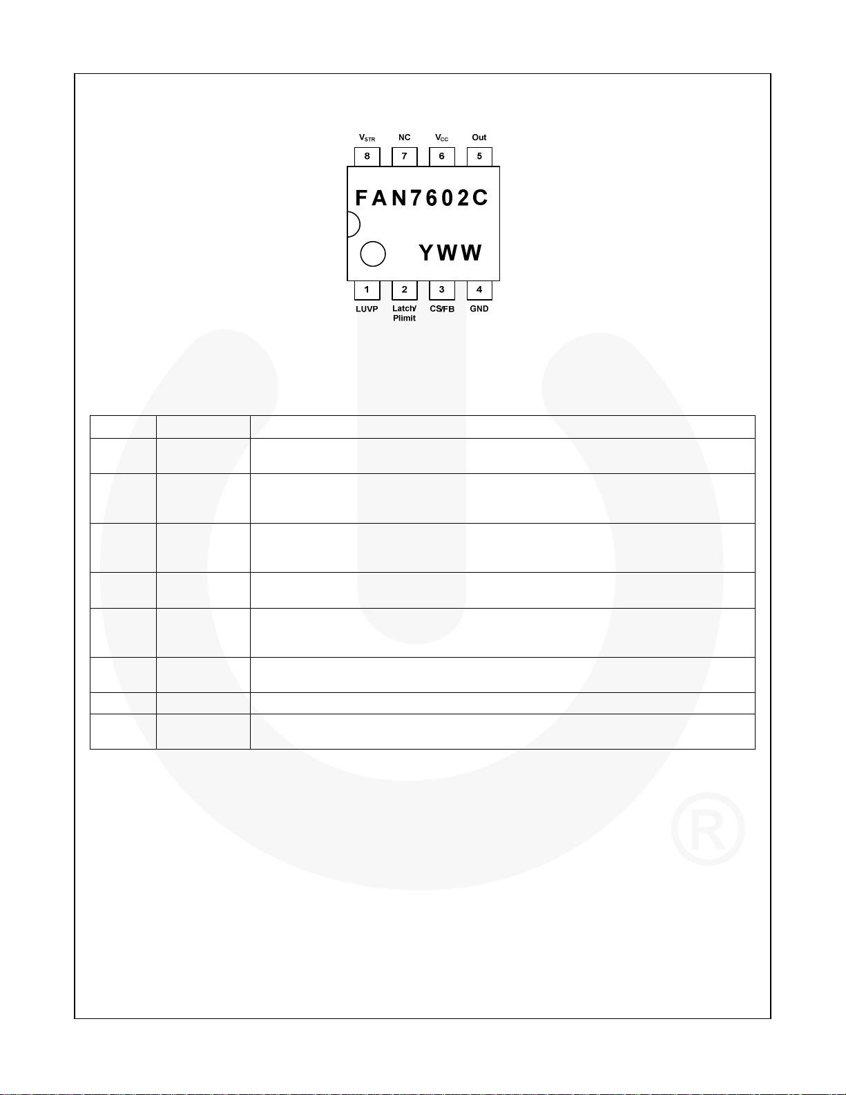
Figure 3. Pin Configuration (Top View)
Pin Definitions
Pin # Name Description
1 LUVP
2 Latch/Plimit
3 CS/FB
4 GND
5 OUT
6 VCC
7 NC
8 V
STR
Line Under-Voltage Protection Pin. This pin is used to protect the set when the input
voltage is lower than the rated input voltage range.
Latch Protection and Power Limit Pin. When the pin voltage exceeds 4V, the latch
protection works. The latch protection is reset when the VCC voltage is lower than 5V. For
the power limit function, the OCP level decreases as the pin voltage increases.
Current Sense and Feedback Pin. This pin is used to sense the MOSFET current for
the current mode PWM and OCP. The output voltage feedback information and the
current sense information are added using an external RC filter.
Ground Pin. This pin is used for the ground potential of all the pins. For proper operation,
the signal ground and the power ground should be separated.
Gate Drive Output Pin. This pin is an output pin to drive an external MOSFET. The peak
sourcing current is 450mA and the peak sinking current is 600mA. For proper operation,
the stray inductance in the gate driving path must be minimized.
Supply Voltage Pin. IC operating current and MOSFET driving current are supplied
using this pin.
No Connection.
Startup Pin. This pin is used to supply IC operating current during IC startup. After
startup, the internal JFET is turned off to reduce power loss.
© 2009 Fairchild Semiconductor Corporation www.fairchildsemi.com
FAN7602C • Rev. 1.0.0 3

FAN7602C — Green Current Mode PWM Controller
Absolute Maximum Ratings
Stresses exceeding the absolute maximum ratings may damage the device. The device may not function or be
operable above the recommended operating conditions and stressing the parts to these levels is not recommended. In
addition, extended exposure to stresses above the recommended operating conditions may affect device reliability.
The absolute maximum ratings are stress ratings only.
Symbol Parameter Min. Max. Unit
VCC Supply Voltage 25 V
IO Output Current -600 +450 mA
V
CS/FB Input Voltage -0.3 20 V
CS/FB
V
LUVP Input Voltage -0.3 10 V
LUVP
V
Latch/Plimit Input Voltage -0.3 10 V
Latch
V
V
STR
TJ
T
Storage Temperature Range -55 +150 °C
STG
PD Power Dissipation 1.2 W
ESD Electrostatic Discharge Capability
Input Voltage 600 V
STR
Junction Temperature +150
Recommended Operating Junction Temperature -40 +150
Human Body Model, JESD22-A114 3.5
Charged Device Model, JESD22-C101 2.0
°C
kV
Thermal Impedance
Symbol Parameter Value Unit
θJA Thermal Resistance
Note:
1. Regarding the test environment and PCB type, please refer to JESD51-2 and JESD51-10.
(1)
, Junction-to-Ambient 8-DIP 100
°C/W
© 2009 Fairchild Semiconductor Corporation www.fairchildsemi.com
FAN7602C • Rev. 1.0.0 4

Electrical Characteristics
VCC = 14V, TA = -25°C~125°C, unless otherwise specified.
Symbol Parameter Condition Min. Typ. Max. Unit
Startup Section
I
V
STR
Under Voltage Lock Out Section
Vth(start) Start Threshold Voltage VCC Increasing 11 12 13 V
Vth(stop) Stop Threshold Voltage VCC Decreasing 7 8 9 V
HY(uvlo) UVLO Hysteresis 3.6 4.0 4.4 V
Supply Current Section
IST Startup Supply Current TA = 25°C 250 320 µA
ICC Operating Supply Current Output Not Switching 1.0 1.5 mA
Soft-Start Section
tSS Soft-Start Time
Startup Current V
STR
(2)
5 10 15 ms
= 30V, TA = 25°C 0.7 1.0 1.4 mA
STR
FAN7602C — Green Current Mode PWM Controller
PWM Section
f
Operating Frequency V
OSC
ᅀf
Frequency Fluctuation
OSC
V
CS/FB Threshold Voltage TA = 25°C 0.9 1.0 1.1 V
CS/FB1
tD Propagation Delay to Output
D
D
MAX
MIN
Maximum Duty Cycle 70 75 80 %
Minimum Duty Cycle 0 %
(2)
±3 kHz
(2)
100 150 ns
Burst Mode Section
V
Burst On Threshold Voltage TA = 25°C 0.84 0.95 1.06 V
CS/FB2
V
Burst Off Threshold Voltage TA = 25°C 0.77 0.88 0.99 V
CS/FB3
Power Limit Section
K
Offset Gain V
Plimit
Output Section
VOH Output Voltage High TA = 25°C, I
VOL Output Voltage Low TA = 25°C, I
tR Rising Time
tF Falling Time
(2)
T
(2)
T
= 0.2V, TA = 25°C 59 65 73 kHz
CS/FB
Latch/Plimit
A
A
= 2V, TA = 25°C 0.12 0.16 0.20
= 100mA 11.5 12.0 14.0 V
source
= 100mA 1.0 2.5 V
sink
= 25°C, CL = 1nF 45 150 ns
= 25°C, CL= 1nF 35 150 ns
Continued on the following page…
© 2009 Fairchild Semiconductor Corporation www.fairchildsemi.com
FAN7602C • Rev. 1.0.0 5

Electrical Characteristics (Continued)
VCC = 14V, TA = -25°C~125°C, unless otherwise specified.
Symbol Parameter Condition Min. Typ. Max. Unit
Protection Section
FAN7602C — Green Current Mode PWM Controller
V
LATCH
t
OLP
t
OLP_ST
V
OLP
V
LUVPoff
V
LUVPon
V
OVP
TSD 170 °C
HYS
Latch Voltage 3.6 4.0 4.4 V
Overload Protection Time
Overload Protection Time at
Startup
(2)
20 22 24 ms
30 37 44 ms
Overload Protection Level 0 0.1 V
Line Under-Voltage Protection
On to Off
Line Under-Voltage Protection
Off to On
TA = 25°C 1.9 2.0 2.1 V
TA = 25°C 1.4 1.5 1.6 V
Over-Voltage Protection TA = 25°C 18 19 20 V
Shutdown Temperature
(2)
60 °C
Note:
2. These parameters, although guaranteed, are not 100% tested in production.
© 2009 Fairchild Semiconductor Corporation www.fairchildsemi.com
FAN7602C • Rev. 1.0.0 6
 Loading...