FAN6863
Highly Integrated Green-Mode PWM Controller
FAN6863 — Highly Integrated Green-Mode PWM Controller
May 2011
Features
Low Standby Power: Under 0.1W
Low Startup Current: 8µA
Low Operating Current at Green Mode: 600µA
Peak-Current Mode Operation with Cycle-by-Cycle
Current Limiting
PWM Frequency Continuously Decreasing with
Burst Mode at Light Loads
V
Over-Voltage Protection (OVP)
DD
Constant Output Power Limit (Full AC Input Range)
Internal Latch Circuit (FAN6863L) for OVP, OTP
SENSE Pin Short-Circuit Protection (SSCP)
Fixed PWM Frequency (65KHz) with Frequency
Hopping
Feedback Open-Loop Protection: 60ms Delay
GATE Output Maximum Voltage Clamp: 13.5V
Soft-Start Time: 5ms
Soft Driving for EMI Improvement
Full Range Frequency Hopping
Internal OTP Sensor with Hysteresis
GATE Driving Capability: 400mA
Description
A highly integrated PWM controller, FAN6863 provides
several features to enhance the performance of flyback
converters. To minimize standby power consumption, a
proprietary Green Mode provides off-time modulation to
continuously decrease the switching frequency under
light-load conditions. Under zero-load conditions, the
power supply enters Burst Mode, which completely
shuts off PWM output. Output restarts just before the
supply voltage drops below the UVLO lower limit. Green
Mode enables power supplies to meet international
power conservation requirements.
The FAN6863 is designed for SMPS and integrates a
frequency-hopping function that helps reduce EMI
emission of a power supply with minimum line filters.
The built-in synchronized slope compensation provides
proprietary sawtooth compensation for constant output
power limit over universal AC input range. The gate
output is clamped at 13.5V to protect the external
MOSFET from over-voltage damage.
Other protection functions include SENSE pin ShortCircuit Protection (SSCP), V
(OVP), and Over-Temperature Protection (OTP). For
OTP, an external NTC thermistor can be applied to
sense the ambient temperature. When V
is activated, an internal latch circuit latches off the
controller. Protection types shown in Table 1.
Table 1. Protection Type
Over-Voltage Protection
DD
OVP or OTP
DD
Applications
General-purpose switched-mode power supplies and
flyback power converters, including:
Power Adapters
Open-Frame SMPS
Part
Number
FAN6863 Latch A/R Latch A/R
FAN6863L Latch Latch Latch A/R
FAN6863R A/R A/R A/R A/R
OVP OLP
OTP /
OTP2
SSCP
SMPS with Surge-Current Output, such as for
Printers, Scanners, Motor Drivers
Ordering Information
Part Number
FAN6863TY
FAN6863LTY
FAN6863RTY
Operating
Temperature Range
-40 to +105°C
Package Packing Method
6-Lead, SuperSOT™-6, JEDEC M0-193,
1.6mm Wide
Tape & Reel
© 2011 Fairchild Semiconductor Corporation www.fairchildsemi.com
FAN6863 • Rev. 1.0.1

Typical Application
FAN6863 — Highly Integrated Green-Mode PWM Controller
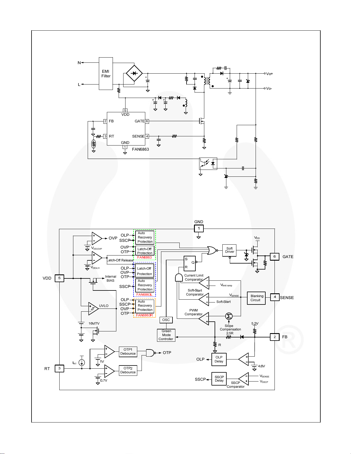
Figure 1. Typical Application
Block Diagram
Figure 2. Block Diagram
© 2011 Fairchild Semiconductor Corporation www.fairchildsemi.com
FAN6863 • Rev. 1.0.1 2

Marking Information
Pin Configuration
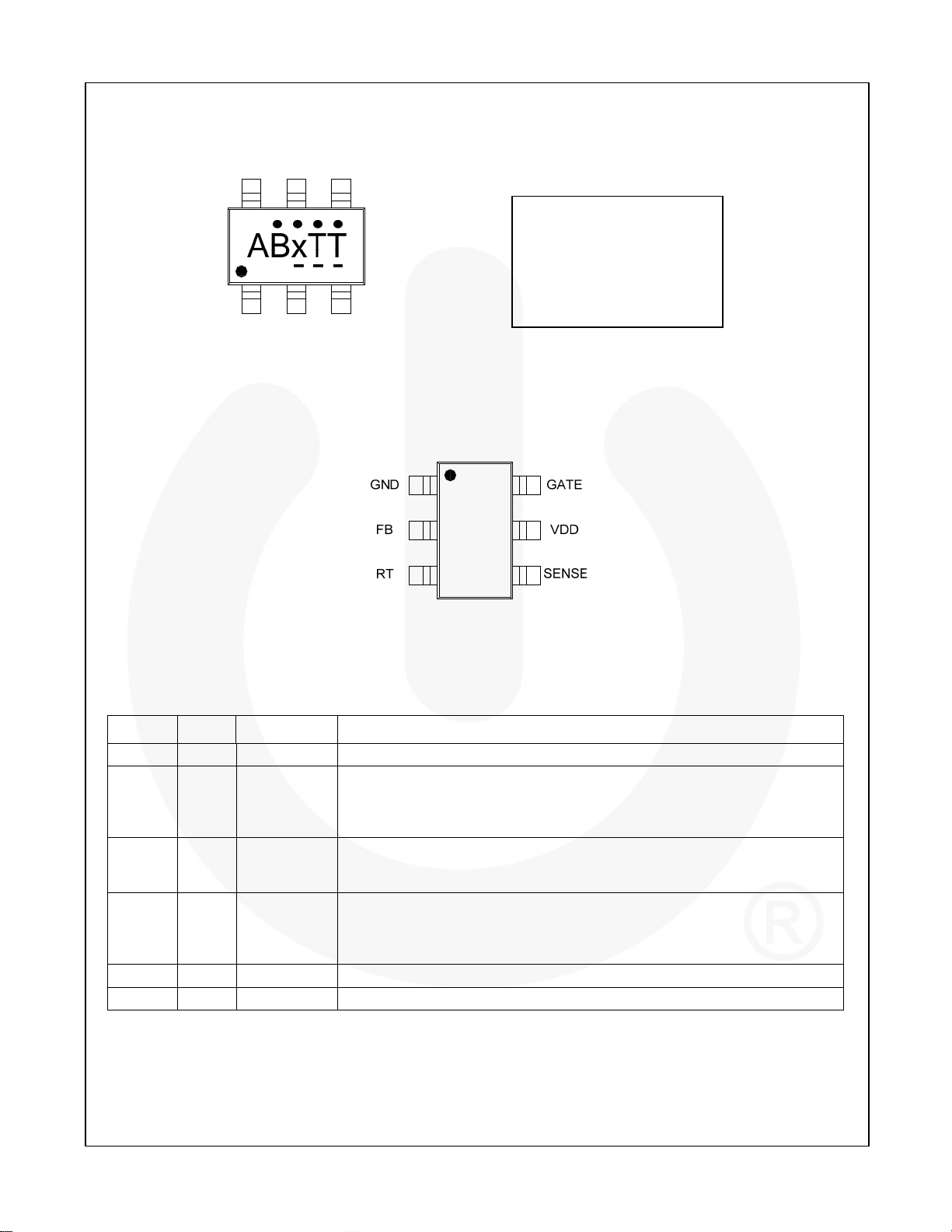
Figure 3. Top Mark
ABx: ABR: FAN6863TY
ABF: FAN6863RTY
ABG: FAN6863LTY
TT: Wafer Lot Code
:
_ _ _: Week Code
Year Code
FAN6863 — Highly Integrated Green-Mode PWM Controller
Figure 4. Pin Configuration
Pin Definitions
Pin # Name Function Description
1 GND Ground Ground.
The FB pin provides the output voltage regulation signal. It provides feedback to
2 FB Feedback
3 RT
4 SENSE Current Sense
5 VDD Power Supply Power supply.
6 GATE Driver Output The totem-pole output driver for driving the power MOSFET.
Temperature
Detection
the internal PWM comparator, so the PWM comparator can control the duty
cycle. This pin also provides over-current protection. Once V
trigger level and last for a long time, the controller stops and restarts.
An external NTC thermistor is connected from this pin to GND pin. The
impedance of the NTC decreases at high temperatures. Once the voltage of the
RT pin drops below a threshold, PWM output is disabled.
This pin senses the voltage across a resistor. When the voltage reaches the
internal threshold, PWM output is disabled and this activates over-current
protection. This pin also provides current amplitude information for CurrentMode control.
is large than
FB
© 2011 Fairchild Semiconductor Corporation www.fairchildsemi.com
FAN6863 • Rev. 1.0.1 3

FAN6863 — Highly Integrated Green-Mode PWM Controller
Absolute Maximum Ratings
Stresses exceeding the absolute maximum ratings may damage the device. The device may not function or be
operable above the recommended operating conditions and stressing the parts to these levels is not recommended.
In addition, extended exposure to stresses above the recommended operating conditions may affect device reliability.
The absolute maximum ratings are stress ratings only. All voltage values, except differential voltages, are given with
respect to GND pin.
Symbol Parameter Min. Max. Unit
VDD Supply Voltage 30 V
VL Input Voltage to FB, SENSE, and RT Pins -0.3 7.0 V
ΘJA Thermal Resistance (Junction-to-Ambient) 247 °C/W
TJ Operating Junction Temperature -40 +125 °C
T
Storage Temperature Range -55 +150 °C
STG
TL Lead Temperature, Wave Soldering, 10 Seconds +260 °C
ESD
Human Body Model, JESD22-A114 5.5
Charge Device Model, JESD22-C101 1.5
kV
Recommended Operating Conditions
The Recommended Operating Conditions table defines the conditions for actual device operation. Recommended
operating conditions are specified to ensure optimal performance to the datasheet specifications. Fairchild does not
recommend exceeding them or designing to Absolute Maximum Ratings.
Symbol Parameter Min. Max. Unit
TA Operating Ambient Temperature -40 +105 °C
© 2011 Fairchild Semiconductor Corporation www.fairchildsemi.com
FAN6863 • Rev. 1.0.1 4

Electrical Characteristics
VDD = 15V and TA = 25°C, unless otherwise noted.
Symbol Parameter Condition Min. Typ. Max. Unit
VDD Section
V
Continuously Operating Voltage 20 V
DD-OP
V
Turn-On Threshold Voltage 15 16 17 V
DD-ON
V
Turn-Off Voltage 6.5 7.0 7.5 V
DD-OFF
V
Threshold Voltage for Latch-Off Release 3 4 5 V
DD-LH
I
Startup Current V
DD-ST
I
DD-OP1
I
DD-OP2
V
DD-OVP
t
D-VDDOVP
I
DD-LH
Operating Supply Current when PWM
Operation
Operating Supply Current when FB< V
FB-ZDC
VDD Over-Voltage Protection
VDD OVP Debounce Time 50 µs
Latch-Off Holding Current
Feedback Input Section
AV Input-Voltage to Current-Sense Attenuation 1/4.0 1/3.5 1/3.0 V/V
ZFB Input Impedance 17 kΩ
V
V
FB Pin Open Voltage 5.2 5.4 5.6 V
FB-OPEN
Threshold Voltage for Open-Loop Protection 4.3 4.6 4.9 V
FB-OLP
t
Open-Loop Protection Delay
D-OLP
t
Secondary Short Circuit Protection Delay
D-SCP
t
Short-Circuit Protection On-Time Detection
ON-SCP
Current Sense Section
tPD Delay to Output 100 250 ns
t
Leading-Edge Blanking Time 200 250 ns
LEB
V
Flat Threshold Voltage for Current Limit Duty>55% 0.6 V
STHFL
V
Valley Threshold Voltage for Current Limit Duty = 0% 0.39 V
STHVA
t
SOFT-START
V
t
ON-SSCP
Period During Startup Time Startup Time 5 ms
Threshold Voltage for SENSE Short-Circuit
SSCP
t
SSCP
Protection
Detect SENSE On Time for SENSE ShortCircuit Protection
Debounce Time for SENSE Short-Circuit
Protection
– 0.16V 8 15 µA
DD-ON
VDD = 20V,
V
= 3V Gate Open
FB
V
= 15V,
DD
V
< V
FB
FB-ZDC
2 mA
600 µA
FAN6863L-Latch,
FAN6863R-Auto
21.5 22.5 23.5 V
Restart
= 5V; FAN6863,
V
DD
FAN6863L Only
FB > V
FB-OLP,
tON < 2.5µs,
= -40 to +105°C
T
A
FB > V
t
< 2.5µs,
ON
T
= -40 to +105°C
A
FB>V
T
= -40 to +105°C
A
t
> 4.5µs,
ON
FB < V
= -40 to +105°C
T
A
FB-OLP
FB-OLP
FB-OLP
,
,
,
t
> 4.5µs,
ON
FB < V
T
= -40 to +105°C
A
FB-OLP
,
70 80 µA
54 60 65 ms
6 7 8 ms
2.5 µs
110 mV
4.4 µs
100 µs
FAN6863 — Highly Integrated Green-Mode PWM Controller
Continued on the following page…
© 2011 Fairchild Semiconductor Corporation www.fairchildsemi.com
FAN6863 • Rev. 1.0.1 5
